
Integration Manual


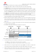


Table Of Contents
- Contents
- 1 System description
- 1.1 Overview
- 1.2 Architecture
- 1.3 Pin-out
- 1.4 Operating modes
- 1.5 Supply interfaces
- 1.5.1 Module supply input (VCC)
- 1.5.1.1 VCC supply requirements
- 1.5.1.2 VCC current consumption in 2G connected mode
- 1.5.1.3 VCC current consumption in 3G connected mode
- 1.5.1.4 VCC current consumption in LTE connected mode
- 1.5.1.5 VCC current consumption in cyclic low power idle mode / active mode
- 1.5.1.6 VCC current consumption in fixed active mode
- 1.5.2 Generic digital interfaces supply output (V_INT)
- 1.5.1 Module supply input (VCC)
- 1.6 System function interfaces
- 1.7 Antenna interfaces
- 1.8 SIM interfaces
- 1.9 Data communication interfaces
- 1.10 eMMC interface
- 1.11 Digital Audio interfaces
- 1.12 ADC interfaces
- 1.13 General Purpose Input/Output
- 1.14 Reserved pins (RSVD)
- 1.15 System features
- 1.15.1 Network indication
- 1.15.2 Jamming detection
- 1.15.3 IP modes of operation
- 1.15.4 Dual stack IPv4 and IPv6
- 1.15.5 Embedded TCP/IP and UDP/IP
- 1.15.6 Embedded FTP and FTPS
- 1.15.7 Embedded HTTP and HTTPS
- 1.15.8 SSL and TLS
- 1.15.9 Firmware update Over AT (FOAT)
- 1.15.10 Firmware update Over The Air (FOTA)
- 1.15.11 Power Saving
- 2 Design-in
- 2.1 Overview
- 2.2 Supply interfaces
- 2.2.1 Module supply (VCC)
- 2.2.1.1 General guidelines for VCC supply circuit selection and design
- 2.2.1.2 Guidelines for VCC supply circuit design using a switching regulator
- 2.2.1.3 Guidelines for VCC supply circuit design using a LDO linear regulator
- 2.2.1.4 Guidelines for VCC supply circuit design using a rechargeable battery
- 2.2.1.5 Guidelines for VCC supply circuit design using a primary battery
- 2.2.1.6 Additional guidelines for VCC supply circuit design
- 2.2.1.7 Guidelines for the external battery charging circuit
- 2.2.1.8 Guidelines for external charging and power path management circuit
- 2.2.1.9 Guidelines for removing VCC supply
- 2.2.1.10 Guidelines for VCC supply layout design
- 2.2.1.11 Guidelines for grounding layout design
- 2.2.2 Generic digital interfaces supply output (V_INT)
- 2.2.1 Module supply (VCC)
- 2.3 System functions interfaces
- 2.4 Antenna interface
- 2.5 SIM interfaces
- 2.6 Data communication interfaces
- 2.7 eMMC interface
- 2.8 Digital Audio interface
- 2.9 ADC interfaces
- 2.10 General Purpose Input/Output
- 2.11 Reserved pins (RSVD)
- 2.12 Module placement
- 2.13 Module footprint and paste mask
- 2.14 Thermal guidelines
- 2.15 Design-in checklist
- 3 Handling and soldering
- 4 Approvals
- 5 Product testing
- 6 FCC Notes
- Appendix
- Glossary
- Related documents
- Revision history
- Contact

TOBY-L3 series - System Integration Manual
TSD-19090601 - R13 System Integration Manual Page 37 of 143
Figure 15 describes the TOBY-L3 series modules’ proper normal switch-off sequence started by means of
the PWR_ON input pin, allowing storage of current parameter settings in the module’s non-volatile memory
and a clean network detach, with the following phases
A low pulse with the appropriate time duration is applied at the PWR_ON input (see TOBY-L3 series
Data Sheet [1], normal graceful switch-off), which is normally set high by an internal pull-up: the module
starts the switch-off routine when the PWR_ON signal is released from the low logical level.
At the end of the switch-off routine, all the digital pins are tri-stated and all the internal voltage
regulators are turned off, including the generic digital interfaces supply (V_INT).
Then, the module remains in power-off mode as long as a switch-on event does not occur (i.e. applying
a suitable low level pulse to the PWR_ON input pin), and enters not-powered mode if the supply is
removed from the VCC pins.
VCC
PWR_ON
RESET_N
V_INT
Int ernal Reset
Syst em St at e
BB Pads St at e
OFF
Tristate / Floating
ON
Operational ->
Tristate
Operational
The module starts
the switch-off routine
VCC
can be removed
Figure 15: Description of TOBY-L3 series power-off sequence, as triggered by PWR_ON input pin
☞ The Internal Reset signal is not available on a module pin, but it is highly recommended to monitor the
V_INT pin to sense the end of the switch-off sequence.
⚠ VCC supply can be removed only after V_INT goes low: an abrupt removal of the VCC supply during
TOBY-L3 series modules normal operations may lead to an unrecoverable faulty state!
☞ The duration of each phase in the TOBY-L3 series modules’ switch-off routines can largely vary
depending on the application / network settings and the concurrent module activities.
1.6.3 Module reset
TOBY-L3 series modules can be properly reset (rebooted) by: