
Integration Manual


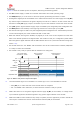


Table Of Contents
- Contents
- 1 System description
- 1.1 Overview
- 1.2 Architecture
- 1.3 Pin-out
- 1.4 Operating modes
- 1.5 Supply interfaces
- 1.5.1 Module supply input (VCC)
- 1.5.1.1 VCC supply requirements
- 1.5.1.2 VCC current consumption in 2G connected mode
- 1.5.1.3 VCC current consumption in 3G connected mode
- 1.5.1.4 VCC current consumption in LTE connected mode
- 1.5.1.5 VCC current consumption in cyclic low power idle mode / active mode
- 1.5.1.6 VCC current consumption in fixed active mode
- 1.5.2 Generic digital interfaces supply output (V_INT)
- 1.5.1 Module supply input (VCC)
- 1.6 System function interfaces
- 1.7 Antenna interfaces
- 1.8 SIM interfaces
- 1.9 Data communication interfaces
- 1.10 eMMC interface
- 1.11 Digital Audio interfaces
- 1.12 ADC interfaces
- 1.13 General Purpose Input/Output
- 1.14 Reserved pins (RSVD)
- 1.15 System features
- 1.15.1 Network indication
- 1.15.2 Jamming detection
- 1.15.3 IP modes of operation
- 1.15.4 Dual stack IPv4 and IPv6
- 1.15.5 Embedded TCP/IP and UDP/IP
- 1.15.6 Embedded FTP and FTPS
- 1.15.7 Embedded HTTP and HTTPS
- 1.15.8 SSL and TLS
- 1.15.9 Firmware update Over AT (FOAT)
- 1.15.10 Firmware update Over The Air (FOTA)
- 1.15.11 Power Saving
- 2 Design-in
- 2.1 Overview
- 2.2 Supply interfaces
- 2.2.1 Module supply (VCC)
- 2.2.1.1 General guidelines for VCC supply circuit selection and design
- 2.2.1.2 Guidelines for VCC supply circuit design using a switching regulator
- 2.2.1.3 Guidelines for VCC supply circuit design using a LDO linear regulator
- 2.2.1.4 Guidelines for VCC supply circuit design using a rechargeable battery
- 2.2.1.5 Guidelines for VCC supply circuit design using a primary battery
- 2.2.1.6 Additional guidelines for VCC supply circuit design
- 2.2.1.7 Guidelines for the external battery charging circuit
- 2.2.1.8 Guidelines for external charging and power path management circuit
- 2.2.1.9 Guidelines for removing VCC supply
- 2.2.1.10 Guidelines for VCC supply layout design
- 2.2.1.11 Guidelines for grounding layout design
- 2.2.2 Generic digital interfaces supply output (V_INT)
- 2.2.1 Module supply (VCC)
- 2.3 System functions interfaces
- 2.4 Antenna interface
- 2.5 SIM interfaces
- 2.6 Data communication interfaces
- 2.7 eMMC interface
- 2.8 Digital Audio interface
- 2.9 ADC interfaces
- 2.10 General Purpose Input/Output
- 2.11 Reserved pins (RSVD)
- 2.12 Module placement
- 2.13 Module footprint and paste mask
- 2.14 Thermal guidelines
- 2.15 Design-in checklist
- 3 Handling and soldering
- 4 Approvals
- 5 Product testing
- 6 FCC Notes
- Appendix
- Glossary
- Related documents
- Revision history
- Contact

TOBY-L3 series - System Integration Manual
TSD-19090601 - R13 System Integration Manual Page 31 of 143
In LTE, the paging period can vary from 320 ms (DRX = 5, i.e. length of 2
5
LTE frames = 32 x 10 ms) up
to 2560 ms (DRX = 8, length of 2
8
LTE frames = 256 x 10 ms).
Figure 9 illustrates a typical example of the module current consumption profile when power saving is
enabled. The module is registered with the network, automatically enters the low power idle mode and
periodically wakes up to active mode to monitor the paging channel for the paging block reception.
~50 ms
IDLE MODE ACTIVE MODE IDLE MODE
Act ive Mode
Enabled
Idle Mode
Enabled
2G case: 0.44-2.09 s
3G case: 0.61-5.09 s
LTE case: 0.27-2.51 s
IDLE MODE
~50 ms
ACTIVE MODE
Time
[s]
Current [mA]
Time
[ms]
Current [mA]
RX
Enabled
0
100
200
0
100
200
Figure 9: VCC current consumption profile with low power mode enabled and module registered with the network: the module
is in low-power idle mode and periodically wakes up to active mode to monitor the paging channel for paging block reception
1.5.1.6 VCC current consumption in fixed active mode
When the USB or the Ethernet SGMII interface is not suspended, the module stays in active mode, ready to
perform its designed operations.
The module processor core is activated during idle mode, and the 19.2 MHz system clock frequency is used.
It would draw more current during the paging period than that in the power saving mode.
Figure 10 illustrates a typical example of the module current consumption profile when power saving is
disabled. In such a case, the module is registered with the network and while active mode is maintained,
the receiver is periodically activated to monitor the paging channel for paging block reception.
It must be noted that the actual current consumption of the module in active mode depends on the specific
concurrent activities performed by the integrated CPU.