
Integration Manual


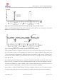


Table Of Contents
- Contents
- 1 System description
- 1.1 Overview
- 1.2 Architecture
- 1.3 Pin-out
- 1.4 Operating modes
- 1.5 Supply interfaces
- 1.5.1 Module supply input (VCC)
- 1.5.1.1 VCC supply requirements
- 1.5.1.2 VCC current consumption in 2G connected mode
- 1.5.1.3 VCC current consumption in 3G connected mode
- 1.5.1.4 VCC current consumption in LTE connected mode
- 1.5.1.5 VCC current consumption in cyclic low power idle mode / active mode
- 1.5.1.6 VCC current consumption in fixed active mode
- 1.5.2 Generic digital interfaces supply output (V_INT)
- 1.5.1 Module supply input (VCC)
- 1.6 System function interfaces
- 1.7 Antenna interfaces
- 1.8 SIM interfaces
- 1.9 Data communication interfaces
- 1.10 eMMC interface
- 1.11 Digital Audio interfaces
- 1.12 ADC interfaces
- 1.13 General Purpose Input/Output
- 1.14 Reserved pins (RSVD)
- 1.15 System features
- 1.15.1 Network indication
- 1.15.2 Jamming detection
- 1.15.3 IP modes of operation
- 1.15.4 Dual stack IPv4 and IPv6
- 1.15.5 Embedded TCP/IP and UDP/IP
- 1.15.6 Embedded FTP and FTPS
- 1.15.7 Embedded HTTP and HTTPS
- 1.15.8 SSL and TLS
- 1.15.9 Firmware update Over AT (FOAT)
- 1.15.10 Firmware update Over The Air (FOTA)
- 1.15.11 Power Saving
- 2 Design-in
- 2.1 Overview
- 2.2 Supply interfaces
- 2.2.1 Module supply (VCC)
- 2.2.1.1 General guidelines for VCC supply circuit selection and design
- 2.2.1.2 Guidelines for VCC supply circuit design using a switching regulator
- 2.2.1.3 Guidelines for VCC supply circuit design using a LDO linear regulator
- 2.2.1.4 Guidelines for VCC supply circuit design using a rechargeable battery
- 2.2.1.5 Guidelines for VCC supply circuit design using a primary battery
- 2.2.1.6 Additional guidelines for VCC supply circuit design
- 2.2.1.7 Guidelines for the external battery charging circuit
- 2.2.1.8 Guidelines for external charging and power path management circuit
- 2.2.1.9 Guidelines for removing VCC supply
- 2.2.1.10 Guidelines for VCC supply layout design
- 2.2.1.11 Guidelines for grounding layout design
- 2.2.2 Generic digital interfaces supply output (V_INT)
- 2.2.1 Module supply (VCC)
- 2.3 System functions interfaces
- 2.4 Antenna interface
- 2.5 SIM interfaces
- 2.6 Data communication interfaces
- 2.7 eMMC interface
- 2.8 Digital Audio interface
- 2.9 ADC interfaces
- 2.10 General Purpose Input/Output
- 2.11 Reserved pins (RSVD)
- 2.12 Module placement
- 2.13 Module footprint and paste mask
- 2.14 Thermal guidelines
- 2.15 Design-in checklist
- 3 Handling and soldering
- 4 Approvals
- 5 Product testing
- 6 FCC Notes
- Appendix
- Glossary
- Related documents
- Revision history
- Contact

TOBY-L3 series - System Integration Manual
TSD-19090601 - R13 System Integration Manual Page 30 of 143
It must be noted that the actual current consumption of the module in LTE connected mode depends also
on the specific concurrent activities performed by the integrated CPU, beside the actual Tx power and
antenna load.
Time
[ms]
Current [mA]
Current consumpt ion value
depends on TX power and
actual ant enna load
1 Slot
1 Resource Block
(0.5 ms)
1 LTE Radio Frame
(10 ms)
0
300
200
100
500
400
600
700
800
900
Figure 8: VCC current consumption profile versus time during LTE connection (TX and RX continuously enabled)
1.5.1.5 VCC current consumption in cyclic low power idle mode / active mode
When both the USB and the Ethernet SGMII interfaces are either suspended or unconnected, the module
enters low power idle mode whenever possible by default on the "50" product version, or if the power
saving configuration is enabled by the AT+UPSV command on the "50" product version (see the TOBY-L3
series AT Commands Manual [2]), or if power state manager is enabled on the "00" product version.
When the module is registered or attached to a network, the module must periodically monitor the paging
channel of the current base station (paging block reception), in accordance with the 2G/3G/LTE system
requirements, even if connected mode is not enabled by the application. When the module monitors the
paging channel, it wakes up to the active mode to then enable the reception of the paging block. In
between, the module switches to low power idle mode. This is known as discontinuous reception (DRX).
The time period between two paging block receptions is defined by the network. This is the paging period
parameter, fixed by the base station through the broadcast channel sent to all users on the same serving
cell:
In 2G, the paging period can vary from 470.8 ms (DRX = 2, length of 2 x 51 2G frames = 2 x 51 x
4.615 ms) up to 2118.4 ms (DRX = 9, length of 9 x 51 2G frames = 9 x 51 x 4.615 ms)
In 3G, the paging period can vary from 640 ms (DRX = 6, i.e. length of 2
6
3G frames = 64 x 10 ms) up
to 5120 ms (DRX = 9, length of 2
9
3G frames = 512 x 10 ms).