
Integration Manual


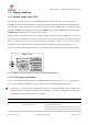
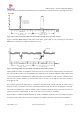

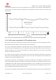

Table Of Contents
- Contents
- 1 System description
- 1.1 Overview
- 1.2 Architecture
- 1.3 Pin-out
- 1.4 Operating modes
- 1.5 Supply interfaces
- 1.5.1 Module supply input (VCC)
- 1.5.1.1 VCC supply requirements
- 1.5.1.2 VCC current consumption in 2G connected mode
- 1.5.1.3 VCC current consumption in 3G connected mode
- 1.5.1.4 VCC current consumption in LTE connected mode
- 1.5.1.5 VCC current consumption in cyclic low power idle mode / active mode
- 1.5.1.6 VCC current consumption in fixed active mode
- 1.5.2 Generic digital interfaces supply output (V_INT)
- 1.5.1 Module supply input (VCC)
- 1.6 System function interfaces
- 1.7 Antenna interfaces
- 1.8 SIM interfaces
- 1.9 Data communication interfaces
- 1.10 eMMC interface
- 1.11 Digital Audio interfaces
- 1.12 ADC interfaces
- 1.13 General Purpose Input/Output
- 1.14 Reserved pins (RSVD)
- 1.15 System features
- 1.15.1 Network indication
- 1.15.2 Jamming detection
- 1.15.3 IP modes of operation
- 1.15.4 Dual stack IPv4 and IPv6
- 1.15.5 Embedded TCP/IP and UDP/IP
- 1.15.6 Embedded FTP and FTPS
- 1.15.7 Embedded HTTP and HTTPS
- 1.15.8 SSL and TLS
- 1.15.9 Firmware update Over AT (FOAT)
- 1.15.10 Firmware update Over The Air (FOTA)
- 1.15.11 Power Saving
- 2 Design-in
- 2.1 Overview
- 2.2 Supply interfaces
- 2.2.1 Module supply (VCC)
- 2.2.1.1 General guidelines for VCC supply circuit selection and design
- 2.2.1.2 Guidelines for VCC supply circuit design using a switching regulator
- 2.2.1.3 Guidelines for VCC supply circuit design using a LDO linear regulator
- 2.2.1.4 Guidelines for VCC supply circuit design using a rechargeable battery
- 2.2.1.5 Guidelines for VCC supply circuit design using a primary battery
- 2.2.1.6 Additional guidelines for VCC supply circuit design
- 2.2.1.7 Guidelines for the external battery charging circuit
- 2.2.1.8 Guidelines for external charging and power path management circuit
- 2.2.1.9 Guidelines for removing VCC supply
- 2.2.1.10 Guidelines for VCC supply layout design
- 2.2.1.11 Guidelines for grounding layout design
- 2.2.2 Generic digital interfaces supply output (V_INT)
- 2.2.1 Module supply (VCC)
- 2.3 System functions interfaces
- 2.4 Antenna interface
- 2.5 SIM interfaces
- 2.6 Data communication interfaces
- 2.7 eMMC interface
- 2.8 Digital Audio interface
- 2.9 ADC interfaces
- 2.10 General Purpose Input/Output
- 2.11 Reserved pins (RSVD)
- 2.12 Module placement
- 2.13 Module footprint and paste mask
- 2.14 Thermal guidelines
- 2.15 Design-in checklist
- 3 Handling and soldering
- 4 Approvals
- 5 Product testing
- 6 FCC Notes
- Appendix
- Glossary
- Related documents
- Revision history
- Contact

TOBY-L3 series - System Integration Manual
TSD-19090601 - R13 System Integration Manual Page 27 of 143
Figure 4 shows an example of the module current consumption profile versus time in 2G single-slot mode.
Time
[ms]
RX
slot
unused
slot
unused
slot
TX
slot
unused
slot
unused
slot
MON
slot
unused
slot
RX
slot
unused
slot
unused
slot
TX
slot
unused
slot
unused
slot
MON
slot
unused
slot
GSM frame
4.615 ms
(1 frame = 8 slot s)
Current [A]
200 mA
60-120 mA
1900 mA
Peak current
depends on TX
power and actual
ant enna load
GSM frame
4.615 ms
(1 frame = 8 slot s)
60-120 m A
10 -40 mA
0.0
1.5
1.0
0.5
2.0
2.5
Figure 4: VCC current consumption profile versus time during a 2G single-slot call (1 TX slot, 1 RX slot)
Figure 5 illustrates VCC voltage profile versus time during a 2G single-slot call, according to the relative
VCC current consumption profile illustrated in Figure 4.
Time [ms]
undershoot
overshoot
ripple
drop
Voltage [mV]
3.8 V
(t yp)
RX
slot
unused
slot
unused
slot
TX
slot
unused
slot
unused
slot
MON
slot
unused
slot
RX
slot
unused
slot
unused
slot
TX
slot
unused
slot
unused
slot
MON
slot
unused
slot
GSM frame
4.615 m s
(1 frame = 8 slot s)
GSM frame
4.615 m s
(1 frame = 8 slot s)
Figure 5: VCC voltage profile versus time during a 2G single-slot call (1 TX slot, 1 RX slot)
When a GPRS connection is established, more than one slot can be used to transmit and/or more than one
slot can be used to receive. The transmitted power depends on the network conditions, which set the peak
current consumption, but following the 3GPP specifications, the maximum Tx RF power is reduced if more
than one slot is used to transmit, so the maximum peak of current is not as high as can be the case with a
2G single-slot call.
If the module transmits in GPRS class 12 in the 850 or 900 MHz bands, at the maximum RF power control
level, the current consumption can reach a quite high peak but lower than the one achievable in 2G single-
slot mode. This happens for 2.307 ms (width of the 4 transmit slots/bursts) with a periodicity of 4.615 ms
(width of 1 frame = 8 slots/bursts), so with a 1/2 duty cycle, according to 2G TDMA.
If the module is in GPRS connected mode in the 1800 or 1900 MHz bands, the current consumption figures
are quite less high than the one in the low bands, due to 3GPP transmitter output power specifications.