
Integration Manual


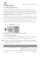
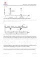

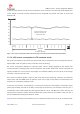

Table Of Contents
- Contents
- 1 System description
- 1.1 Overview
- 1.2 Architecture
- 1.3 Pin-out
- 1.4 Operating modes
- 1.5 Supply interfaces
- 1.5.1 Module supply input (VCC)
- 1.5.1.1 VCC supply requirements
- 1.5.1.2 VCC current consumption in 2G connected mode
- 1.5.1.3 VCC current consumption in 3G connected mode
- 1.5.1.4 VCC current consumption in LTE connected mode
- 1.5.1.5 VCC current consumption in cyclic low power idle mode / active mode
- 1.5.1.6 VCC current consumption in fixed active mode
- 1.5.2 Generic digital interfaces supply output (V_INT)
- 1.5.1 Module supply input (VCC)
- 1.6 System function interfaces
- 1.7 Antenna interfaces
- 1.8 SIM interfaces
- 1.9 Data communication interfaces
- 1.10 eMMC interface
- 1.11 Digital Audio interfaces
- 1.12 ADC interfaces
- 1.13 General Purpose Input/Output
- 1.14 Reserved pins (RSVD)
- 1.15 System features
- 1.15.1 Network indication
- 1.15.2 Jamming detection
- 1.15.3 IP modes of operation
- 1.15.4 Dual stack IPv4 and IPv6
- 1.15.5 Embedded TCP/IP and UDP/IP
- 1.15.6 Embedded FTP and FTPS
- 1.15.7 Embedded HTTP and HTTPS
- 1.15.8 SSL and TLS
- 1.15.9 Firmware update Over AT (FOAT)
- 1.15.10 Firmware update Over The Air (FOTA)
- 1.15.11 Power Saving
- 2 Design-in
- 2.1 Overview
- 2.2 Supply interfaces
- 2.2.1 Module supply (VCC)
- 2.2.1.1 General guidelines for VCC supply circuit selection and design
- 2.2.1.2 Guidelines for VCC supply circuit design using a switching regulator
- 2.2.1.3 Guidelines for VCC supply circuit design using a LDO linear regulator
- 2.2.1.4 Guidelines for VCC supply circuit design using a rechargeable battery
- 2.2.1.5 Guidelines for VCC supply circuit design using a primary battery
- 2.2.1.6 Additional guidelines for VCC supply circuit design
- 2.2.1.7 Guidelines for the external battery charging circuit
- 2.2.1.8 Guidelines for external charging and power path management circuit
- 2.2.1.9 Guidelines for removing VCC supply
- 2.2.1.10 Guidelines for VCC supply layout design
- 2.2.1.11 Guidelines for grounding layout design
- 2.2.2 Generic digital interfaces supply output (V_INT)
- 2.2.1 Module supply (VCC)
- 2.3 System functions interfaces
- 2.4 Antenna interface
- 2.5 SIM interfaces
- 2.6 Data communication interfaces
- 2.7 eMMC interface
- 2.8 Digital Audio interface
- 2.9 ADC interfaces
- 2.10 General Purpose Input/Output
- 2.11 Reserved pins (RSVD)
- 2.12 Module placement
- 2.13 Module footprint and paste mask
- 2.14 Thermal guidelines
- 2.15 Design-in checklist
- 3 Handling and soldering
- 4 Approvals
- 5 Product testing
- 6 FCC Notes
- Appendix
- Glossary
- Related documents
- Revision history
- Contact

TOBY-L3 series - System Integration Manual
TSD-19090601 - R13 System Integration Manual Page 26 of 143
functional until the VCC voltage is inside the extended operating
range limits.
VCC average current
Support with adequate margin the
highest averaged VCC current
consumption value in connected mode
conditions
The maximum average current consumption can be greater than
the specified value according to the actual antenna mismatching,
temperature and supply voltage.
Sections 1.5.1.2, 1.5.1.3 and 1.5.1.4 describe the current
consumption profiles in 2G, 3G and LTE connected modes.
VCC peak current
Support with margin the highest peak
VCC current consumption value in
connected mode conditions
The specified maximum peak of current consumption occurs
during the GSM single transmit slot in 850/900 MHz connected
mode, in case of a mismatched antenna.
Section 1.5.1.2 describes 2G Tx peak/pulse current.
VCC voltage drop
during 2G Tx slots
Lower than 400 mV
Supply voltage drop values greater than recommended during 2G
TDMA transmission slots directly affect the RF compliance with
the applicable certification schemes.
Figure 5 describes supply voltage drop during 2G Tx slots.
VCC voltage ripple
during 2G/3G/LTE Tx
Noise in the supply must be minimized
High supply voltage ripple values during LTE/3G/2G RF
transmissions in connected mode directly affect the RF
compliance with applicable certification schemes.
Figure 5 describes supply voltage ripple during RF Tx.
VCC under/over-shoot
at start/end of Tx slots
Absent or at least minimized
Supply voltage under-shoot or over-shoot at the start or the end
of 2G TDMA transmission slots directly affect the RF compliance
with the applicable certification schemes.
Figure 5 describes supply voltage under/over-shoot
Table 7: Summary of VCC modules supply requirements
1.5.1.2 VCC current consumption in 2G connected mode
When a GSM call is established, the VCC module current consumption is determined by the current
consumption profile typical of the GSM transmitting and receiving bursts.
The peak of current consumption during a transmission slot is strictly dependent on the RF transmitted
power, which is regulated by the network (the current base station). The transmitted power in the transmit
slot is also the more relevant factor for determining the average current consumption.
If the module is transmitting in 2G single-slot mode in the 850 or 900 MHz bands, at the maximum RF
power level (approximately 2 W or 33 dBm in the allocated transmit slot/burst) the current consumption
can reach an upper peak for 576.9 µs (width of the transmit slot/burst) with a periodicity of 4.615 ms (width
of 1 frame = 8 slots/burst), so with a 1/8 duty cycle according to GSM TDMA (Time Division Multiple Access).
If the module is transmitting in 2G single-slot mode in the 1800 or 1900 MHz bands, the current
consumption figures are considerably lower than the one in the low bands, due to the 3GPP transmitter
output power specifications.
During a GSM call, current consumption is not so significantly high in receiving or in monitor bursts and is
low in the inactive unused bursts.