
Integration Manual


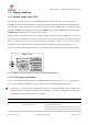
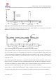


Table Of Contents
- Contents
- 1 System description
- 1.1 Overview
- 1.2 Architecture
- 1.3 Pin-out
- 1.4 Operating modes
- 1.5 Supply interfaces
- 1.5.1 Module supply input (VCC)
- 1.5.1.1 VCC supply requirements
- 1.5.1.2 VCC current consumption in 2G connected mode
- 1.5.1.3 VCC current consumption in 3G connected mode
- 1.5.1.4 VCC current consumption in LTE connected mode
- 1.5.1.5 VCC current consumption in cyclic low power idle mode / active mode
- 1.5.1.6 VCC current consumption in fixed active mode
- 1.5.2 Generic digital interfaces supply output (V_INT)
- 1.5.1 Module supply input (VCC)
- 1.6 System function interfaces
- 1.7 Antenna interfaces
- 1.8 SIM interfaces
- 1.9 Data communication interfaces
- 1.10 eMMC interface
- 1.11 Digital Audio interfaces
- 1.12 ADC interfaces
- 1.13 General Purpose Input/Output
- 1.14 Reserved pins (RSVD)
- 1.15 System features
- 1.15.1 Network indication
- 1.15.2 Jamming detection
- 1.15.3 IP modes of operation
- 1.15.4 Dual stack IPv4 and IPv6
- 1.15.5 Embedded TCP/IP and UDP/IP
- 1.15.6 Embedded FTP and FTPS
- 1.15.7 Embedded HTTP and HTTPS
- 1.15.8 SSL and TLS
- 1.15.9 Firmware update Over AT (FOAT)
- 1.15.10 Firmware update Over The Air (FOTA)
- 1.15.11 Power Saving
- 2 Design-in
- 2.1 Overview
- 2.2 Supply interfaces
- 2.2.1 Module supply (VCC)
- 2.2.1.1 General guidelines for VCC supply circuit selection and design
- 2.2.1.2 Guidelines for VCC supply circuit design using a switching regulator
- 2.2.1.3 Guidelines for VCC supply circuit design using a LDO linear regulator
- 2.2.1.4 Guidelines for VCC supply circuit design using a rechargeable battery
- 2.2.1.5 Guidelines for VCC supply circuit design using a primary battery
- 2.2.1.6 Additional guidelines for VCC supply circuit design
- 2.2.1.7 Guidelines for the external battery charging circuit
- 2.2.1.8 Guidelines for external charging and power path management circuit
- 2.2.1.9 Guidelines for removing VCC supply
- 2.2.1.10 Guidelines for VCC supply layout design
- 2.2.1.11 Guidelines for grounding layout design
- 2.2.2 Generic digital interfaces supply output (V_INT)
- 2.2.1 Module supply (VCC)
- 2.3 System functions interfaces
- 2.4 Antenna interface
- 2.5 SIM interfaces
- 2.6 Data communication interfaces
- 2.7 eMMC interface
- 2.8 Digital Audio interface
- 2.9 ADC interfaces
- 2.10 General Purpose Input/Output
- 2.11 Reserved pins (RSVD)
- 2.12 Module placement
- 2.13 Module footprint and paste mask
- 2.14 Thermal guidelines
- 2.15 Design-in checklist
- 3 Handling and soldering
- 4 Approvals
- 5 Product testing
- 6 FCC Notes
- Appendix
- Glossary
- Related documents
- Revision history
- Contact

TOBY-L3 series - System Integration Manual
TSD-19090601 - R13 System Integration Manual Page 24 of 143
Power off
Connected
Sleep
Active
Booting
Apply VCC
power supply
Switch OFF:
1). AT+CPWROFF
2). RESET_N (hardware reset)
3). Low pulse on PWR_ON
Boot up
finished
Incoming/outgoing call or
other dedicated device
network communication
No LTE/3G/2G data connection
in progress, Call terminated,
communication dropped
Any wake up event described
in the module operating
modes summary table above
If power saving is enabled
and there is no activity for
a defined time interval
Not powered
Remove VCC
power supply
Switch ON:
1). PWR_ON
Download
Firmware
Download
Boot With Recovery
Switch ON with the
Pin TX2 pull up to high
Figure 2: TOBY-L3 series operating modes transition