
Integration Manual
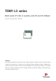
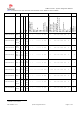
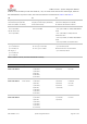
Table Of Contents
- Contents
- 1 System description
- 1.1 Overview
- 1.2 Architecture
- 1.3 Pin-out
- 1.4 Operating modes
- 1.5 Supply interfaces
- 1.5.1 Module supply input (VCC)
- 1.5.1.1 VCC supply requirements
- 1.5.1.2 VCC current consumption in 2G connected mode
- 1.5.1.3 VCC current consumption in 3G connected mode
- 1.5.1.4 VCC current consumption in LTE connected mode
- 1.5.1.5 VCC current consumption in cyclic low power idle mode / active mode
- 1.5.1.6 VCC current consumption in fixed active mode
- 1.5.2 Generic digital interfaces supply output (V_INT)
- 1.5.1 Module supply input (VCC)
- 1.6 System function interfaces
- 1.7 Antenna interfaces
- 1.8 SIM interfaces
- 1.9 Data communication interfaces
- 1.10 eMMC interface
- 1.11 Digital Audio interfaces
- 1.12 ADC interfaces
- 1.13 General Purpose Input/Output
- 1.14 Reserved pins (RSVD)
- 1.15 System features
- 1.15.1 Network indication
- 1.15.2 Jamming detection
- 1.15.3 IP modes of operation
- 1.15.4 Dual stack IPv4 and IPv6
- 1.15.5 Embedded TCP/IP and UDP/IP
- 1.15.6 Embedded FTP and FTPS
- 1.15.7 Embedded HTTP and HTTPS
- 1.15.8 SSL and TLS
- 1.15.9 Firmware update Over AT (FOAT)
- 1.15.10 Firmware update Over The Air (FOTA)
- 1.15.11 Power Saving
- 2 Design-in
- 2.1 Overview
- 2.2 Supply interfaces
- 2.2.1 Module supply (VCC)
- 2.2.1.1 General guidelines for VCC supply circuit selection and design
- 2.2.1.2 Guidelines for VCC supply circuit design using a switching regulator
- 2.2.1.3 Guidelines for VCC supply circuit design using a LDO linear regulator
- 2.2.1.4 Guidelines for VCC supply circuit design using a rechargeable battery
- 2.2.1.5 Guidelines for VCC supply circuit design using a primary battery
- 2.2.1.6 Additional guidelines for VCC supply circuit design
- 2.2.1.7 Guidelines for the external battery charging circuit
- 2.2.1.8 Guidelines for external charging and power path management circuit
- 2.2.1.9 Guidelines for removing VCC supply
- 2.2.1.10 Guidelines for VCC supply layout design
- 2.2.1.11 Guidelines for grounding layout design
- 2.2.2 Generic digital interfaces supply output (V_INT)
- 2.2.1 Module supply (VCC)
- 2.3 System functions interfaces
- 2.4 Antenna interface
- 2.5 SIM interfaces
- 2.6 Data communication interfaces
- 2.7 eMMC interface
- 2.8 Digital Audio interface
- 2.9 ADC interfaces
- 2.10 General Purpose Input/Output
- 2.11 Reserved pins (RSVD)
- 2.12 Module placement
- 2.13 Module footprint and paste mask
- 2.14 Thermal guidelines
- 2.15 Design-in checklist
- 3 Handling and soldering
- 4 Approvals
- 5 Product testing
- 6 FCC Notes
- Appendix
- Glossary
- Related documents
- Revision history
- Contact

TOBY-L3 series - System Integration Manual
TSD-19090601 - R13 Page 2 of 143
Document Information
Title
TOBY-L3 series
Subtitle
Multi-mode LTE (Cat 4) modules with 3G and 2G fallback
Document type
System Integration Manual
Document number
TSD-19090601
Revision and date
R13
24-Jan-2022
Disclosure Restriction
Product status
Corresponding content status
Functional Sample
Draft
For functional testing. Revised and supplementary data will be published later.
In Development /
Prototype
Objective Specification
Target values. Revised and supplementary data will be published later.
Engineering Sample
Advance Information
Data based on early testing. Revised and supplementary data will be published later.
Initial Production
Early Production Information
Data from product verification. Revised and supplementary data may be published later.
Mass Production /
End of Life
Production Information
Document contains the final product specification.
This document applies to the following products:
Product name
Type number
Modem version
Application version
PCN reference
Product status
TOBY-L3104
TOBY-L3104-50A-00-00
M31.01.01.03.11
A31.50.20.11
Mass Production
TOBY-L3104-50A-00-01
M31.01.01.03.12
A31.50.20.12
TSD-21121301
Mass Production
TOBY-L3104-50B-00-00
M30.01.01.02.11
A30.50.20.11
Mass Production
TOBY-L3104-50B-00-01
M30.01.01.02.14
A30.50.20.14
TSD-21121302
Mass Production
TOBY-L3204
TOBY-L3204-50A-00-00
M31.02.01.03.12
A31.50.20.12
Mass Production
TOBY-L3204-50B-00-00
M30.02.01.03.12
A30.50.20.12
Mass Production
TOBY-L3404
TOBY-L3404-50A-00-00
M31.04.01.03.12
A31.50.20.12
Mass Production
TOBY-L3404-50B-00-00
M30.04.01.03.12
A30.50.20.12
Mass Production
TOBY-L3904
TOBY-L3904-50A-00-00
M31.09.00.03.14
A31.50.20.14
Mass Production
TOBY-L3904-50B-00-00
M30.09.00.05.08
A30.50.20.08
Mass Production
TOBY-L3904-50A-01-00
M31.09.01.01.10
A31.50.20.10
Mass Production
TOBY-L3904-50A-01-01
M31.09.01.03.13
A31.50.20.13
TSD-21090101
Mass Production
TOBY-L3904-50A-01-02
M31.09.01.03.14
A31.50.20.14
TSD-21101501
Mass Production
TOBY-L3904-50B-01-00
M30.09.01.02.13
A30.50.20.13
Mass Production
TOBY-L3904-50A-11-00
M31.09.01.03.01
A31.00.12.01
Mass Production