
Integration Manual
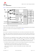
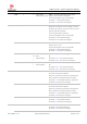
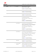


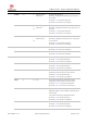
Table Of Contents
- Contents
- 1 System description
- 1.1 Overview
- 1.2 Architecture
- 1.3 Pin-out
- 1.4 Operating modes
- 1.5 Supply interfaces
- 1.5.1 Module supply input (VCC)
- 1.5.1.1 VCC supply requirements
- 1.5.1.2 VCC current consumption in 2G connected mode
- 1.5.1.3 VCC current consumption in 3G connected mode
- 1.5.1.4 VCC current consumption in LTE connected mode
- 1.5.1.5 VCC current consumption in cyclic low power idle mode / active mode
- 1.5.1.6 VCC current consumption in fixed active mode
- 1.5.2 Generic digital interfaces supply output (V_INT)
- 1.5.1 Module supply input (VCC)
- 1.6 System function interfaces
- 1.7 Antenna interfaces
- 1.8 SIM interfaces
- 1.9 Data communication interfaces
- 1.10 eMMC interface
- 1.11 Digital Audio interfaces
- 1.12 ADC interfaces
- 1.13 General Purpose Input/Output
- 1.14 Reserved pins (RSVD)
- 1.15 System features
- 1.15.1 Network indication
- 1.15.2 Jamming detection
- 1.15.3 IP modes of operation
- 1.15.4 Dual stack IPv4 and IPv6
- 1.15.5 Embedded TCP/IP and UDP/IP
- 1.15.6 Embedded FTP and FTPS
- 1.15.7 Embedded HTTP and HTTPS
- 1.15.8 SSL and TLS
- 1.15.9 Firmware update Over AT (FOAT)
- 1.15.10 Firmware update Over The Air (FOTA)
- 1.15.11 Power Saving
- 2 Design-in
- 2.1 Overview
- 2.2 Supply interfaces
- 2.2.1 Module supply (VCC)
- 2.2.1.1 General guidelines for VCC supply circuit selection and design
- 2.2.1.2 Guidelines for VCC supply circuit design using a switching regulator
- 2.2.1.3 Guidelines for VCC supply circuit design using a LDO linear regulator
- 2.2.1.4 Guidelines for VCC supply circuit design using a rechargeable battery
- 2.2.1.5 Guidelines for VCC supply circuit design using a primary battery
- 2.2.1.6 Additional guidelines for VCC supply circuit design
- 2.2.1.7 Guidelines for the external battery charging circuit
- 2.2.1.8 Guidelines for external charging and power path management circuit
- 2.2.1.9 Guidelines for removing VCC supply
- 2.2.1.10 Guidelines for VCC supply layout design
- 2.2.1.11 Guidelines for grounding layout design
- 2.2.2 Generic digital interfaces supply output (V_INT)
- 2.2.1 Module supply (VCC)
- 2.3 System functions interfaces
- 2.4 Antenna interface
- 2.5 SIM interfaces
- 2.6 Data communication interfaces
- 2.7 eMMC interface
- 2.8 Digital Audio interface
- 2.9 ADC interfaces
- 2.10 General Purpose Input/Output
- 2.11 Reserved pins (RSVD)
- 2.12 Module placement
- 2.13 Module footprint and paste mask
- 2.14 Thermal guidelines
- 2.15 Design-in checklist
- 3 Handling and soldering
- 4 Approvals
- 5 Product testing
- 6 FCC Notes
- Appendix
- Glossary
- Related documents
- Revision history
- Contact

TOBY-L3 series - System Integration Manual
TSD-19090601 - R13 System Integration Manual Page 15 of 143
Function
Pin Name
Pin No
I/O
Description
Remarks
SIM_IO
57
I/O
SIM data
Data input/output for 1.8 V / 3 V SIM.
Internal 4.7 k pull-up to VSIM.
See section 1.8 for functional description.
See section 2.5 for external circuit design-in.
SIM_CLK
56
O
SIM clock
3.9 MHz clock output for 1.8 V / 3 V SIM.
See section 1.8 for functional description.
See section 2.5 for external circuit design-in.
SIM_RST
58
O
SIM reset
Reset output for 1.8 V / 3 V SIM.
See section 1.8 for functional description.
See section 2.5 for external circuit design-in.
USB
VUSB_DET
4
I
USB detect input
VBUS (5 V typical) must be connected to this pin to enable
the module USB device interface.
Test-Point for diagnostic / FW update access is
recommended.
See section 1.8.1 for functional description.
See section 2.6.1 for external circuit design-in.
USB_D–
27
I/O
USB High-Speed 2.0
diff. transceiver (–)
90 nominal differential impedance (Z
0
).
30 nominal common mode impedance (Z
CM
).
Pull-up or pull-down resistors and external series resistors as
required by the USB 2.0 specs [4] are part of the USB pin
driver and need not be provided externally.
Test-Point for diagnostic / FW update access is
recommended.
See section 1.9.1 for functional description.
See section 2.6.1 for external circuit design-in.
USB_D+
28
I/O
USB High-Speed 2.0
diff. transceiver (+)
90 nominal differential impedance (Z
0
).
30 nominal common mode impedance (Z
CM
).
Pull-up or pull-down resistors and external series resistors as
required by the USB 2.0 specs [4] are part of the USB pin
driver and need not be provided externally.
Test-Point for diagnostic / FW update access is
recommended.
See section 1.9.1 for functional description.
See section 2.6.1 for external circuit design-in.
USB_ID
168
I
USB device
identification
Pin for ID resistance measurement.
See section 1.9.1 for functional description.
See section 2.6.1 for external circuit design-in.
UART0
RXD
17
O /
O
UART0 data output /
SPI1 Master Output
Slave Input
1.8 V output, Circuit 104 (RXD) in ITU-T V.24.
Alternatively configurable as SPI1 Master Output Slave Input.
Test-Point for diagnostic access recommended.
See section 1.9.2 for functional description.
See section 2.6.2 for external circuit design-in.