
Integration Manual


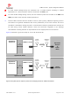
Table Of Contents
- Contents
- 1 System description
- 1.1 Overview
- 1.2 Architecture
- 1.3 Pin-out
- 1.4 Operating modes
- 1.5 Supply interfaces
- 1.5.1 Module supply input (VCC)
- 1.5.1.1 VCC supply requirements
- 1.5.1.2 VCC current consumption in 2G connected mode
- 1.5.1.3 VCC current consumption in 3G connected mode
- 1.5.1.4 VCC current consumption in LTE connected mode
- 1.5.1.5 VCC current consumption in cyclic low power idle mode / active mode
- 1.5.1.6 VCC current consumption in fixed active mode
- 1.5.2 Generic digital interfaces supply output (V_INT)
- 1.5.1 Module supply input (VCC)
- 1.6 System function interfaces
- 1.7 Antenna interfaces
- 1.8 SIM interfaces
- 1.9 Data communication interfaces
- 1.10 eMMC interface
- 1.11 Digital Audio interfaces
- 1.12 ADC interfaces
- 1.13 General Purpose Input/Output
- 1.14 Reserved pins (RSVD)
- 1.15 System features
- 1.15.1 Network indication
- 1.15.2 Jamming detection
- 1.15.3 IP modes of operation
- 1.15.4 Dual stack IPv4 and IPv6
- 1.15.5 Embedded TCP/IP and UDP/IP
- 1.15.6 Embedded FTP and FTPS
- 1.15.7 Embedded HTTP and HTTPS
- 1.15.8 SSL and TLS
- 1.15.9 Firmware update Over AT (FOAT)
- 1.15.10 Firmware update Over The Air (FOTA)
- 1.15.11 Power Saving
- 2 Design-in
- 2.1 Overview
- 2.2 Supply interfaces
- 2.2.1 Module supply (VCC)
- 2.2.1.1 General guidelines for VCC supply circuit selection and design
- 2.2.1.2 Guidelines for VCC supply circuit design using a switching regulator
- 2.2.1.3 Guidelines for VCC supply circuit design using a LDO linear regulator
- 2.2.1.4 Guidelines for VCC supply circuit design using a rechargeable battery
- 2.2.1.5 Guidelines for VCC supply circuit design using a primary battery
- 2.2.1.6 Additional guidelines for VCC supply circuit design
- 2.2.1.7 Guidelines for the external battery charging circuit
- 2.2.1.8 Guidelines for external charging and power path management circuit
- 2.2.1.9 Guidelines for removing VCC supply
- 2.2.1.10 Guidelines for VCC supply layout design
- 2.2.1.11 Guidelines for grounding layout design
- 2.2.2 Generic digital interfaces supply output (V_INT)
- 2.2.1 Module supply (VCC)
- 2.3 System functions interfaces
- 2.4 Antenna interface
- 2.5 SIM interfaces
- 2.6 Data communication interfaces
- 2.7 eMMC interface
- 2.8 Digital Audio interface
- 2.9 ADC interfaces
- 2.10 General Purpose Input/Output
- 2.11 Reserved pins (RSVD)
- 2.12 Module placement
- 2.13 Module footprint and paste mask
- 2.14 Thermal guidelines
- 2.15 Design-in checklist
- 3 Handling and soldering
- 4 Approvals
- 5 Product testing
- 6 FCC Notes
- Appendix
- Glossary
- Related documents
- Revision history
- Contact

TSD-19090601 - R13 Appendix Page 140 of 143
Abbreviation
Definition
QPSK
Quadrature Phase Shift Keying
RF
Radio Frequency
RGMII
Reduced Gigabit Media Independent Interface
RMII
Reduced Media Independent Interface
RSE
Radiated Spurious Emission
RTC
Real Time Clock
SAW
Surface Acoustic Wave
SDIO
Secure Digital Input Output
SDN / PCN / IN
Sample Delivery Note / Product Change Notification / Information Note
SGMII
Serial Gigabit Media Independent Interface
SIM
Subscriber Identification Module
SMS
Short Message Service
SPI
Serial Peripheral Interface
SRF
Self Resonant Frequency
SSL
Secure Socket Layer
TBD
To Be Defined
TCP
Transmission Control Protocol
TDD
Time Division Duplex
TDMA
Time Division Multiple Access
TIS
Total Isotropic Sensitivity
TP
Test-Point
TRP
Total Radiated Power
UART
Universal Asynchronous Receiver-Transmitter
UICC
Universal Integrated Circuit Card
UL
Up-Link (Transmission)
UMTS
Universal Mobile Telecommunications System
USB
Universal Serial Bus
VoLTE
Voice over LTE
VSWR
Voltage Standing Wave Ratio
W-CDMA
Wideband Code Division Multiple Access
Wi-Fi
Wireless Local Area Network (IEEE 802.11 short range radio technology)
WLAN
Wireless Local Area Network (IEEE 802.11 short range radio technology)
WWAN
Wireless Wide Area Network (GSM / UMTS / LTE cellular radio technology)