
Integration Manual


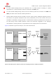
Table Of Contents
- Contents
- 1 System description
- 1.1 Overview
- 1.2 Architecture
- 1.3 Pin-out
- 1.4 Operating modes
- 1.5 Supply interfaces
- 1.5.1 Module supply input (VCC)
- 1.5.1.1 VCC supply requirements
- 1.5.1.2 VCC current consumption in 2G connected mode
- 1.5.1.3 VCC current consumption in 3G connected mode
- 1.5.1.4 VCC current consumption in LTE connected mode
- 1.5.1.5 VCC current consumption in cyclic low power idle mode / active mode
- 1.5.1.6 VCC current consumption in fixed active mode
- 1.5.2 Generic digital interfaces supply output (V_INT)
- 1.5.1 Module supply input (VCC)
- 1.6 System function interfaces
- 1.7 Antenna interfaces
- 1.8 SIM interfaces
- 1.9 Data communication interfaces
- 1.10 eMMC interface
- 1.11 Digital Audio interfaces
- 1.12 ADC interfaces
- 1.13 General Purpose Input/Output
- 1.14 Reserved pins (RSVD)
- 1.15 System features
- 1.15.1 Network indication
- 1.15.2 Jamming detection
- 1.15.3 IP modes of operation
- 1.15.4 Dual stack IPv4 and IPv6
- 1.15.5 Embedded TCP/IP and UDP/IP
- 1.15.6 Embedded FTP and FTPS
- 1.15.7 Embedded HTTP and HTTPS
- 1.15.8 SSL and TLS
- 1.15.9 Firmware update Over AT (FOAT)
- 1.15.10 Firmware update Over The Air (FOTA)
- 1.15.11 Power Saving
- 2 Design-in
- 2.1 Overview
- 2.2 Supply interfaces
- 2.2.1 Module supply (VCC)
- 2.2.1.1 General guidelines for VCC supply circuit selection and design
- 2.2.1.2 Guidelines for VCC supply circuit design using a switching regulator
- 2.2.1.3 Guidelines for VCC supply circuit design using a LDO linear regulator
- 2.2.1.4 Guidelines for VCC supply circuit design using a rechargeable battery
- 2.2.1.5 Guidelines for VCC supply circuit design using a primary battery
- 2.2.1.6 Additional guidelines for VCC supply circuit design
- 2.2.1.7 Guidelines for the external battery charging circuit
- 2.2.1.8 Guidelines for external charging and power path management circuit
- 2.2.1.9 Guidelines for removing VCC supply
- 2.2.1.10 Guidelines for VCC supply layout design
- 2.2.1.11 Guidelines for grounding layout design
- 2.2.2 Generic digital interfaces supply output (V_INT)
- 2.2.1 Module supply (VCC)
- 2.3 System functions interfaces
- 2.4 Antenna interface
- 2.5 SIM interfaces
- 2.6 Data communication interfaces
- 2.7 eMMC interface
- 2.8 Digital Audio interface
- 2.9 ADC interfaces
- 2.10 General Purpose Input/Output
- 2.11 Reserved pins (RSVD)
- 2.12 Module placement
- 2.13 Module footprint and paste mask
- 2.14 Thermal guidelines
- 2.15 Design-in checklist
- 3 Handling and soldering
- 4 Approvals
- 5 Product testing
- 6 FCC Notes
- Appendix
- Glossary
- Related documents
- Revision history
- Contact

TSD-19090601 - R13 Appendix Page 139 of 143
Abbreviation
Definition
FTP
File Transfer Protocol
FW
Firmware
GMSK
Gaussian Minimum-Shift Keying modulation
GND
Ground
GNSS
Global Navigation Satellite System
GPIO
General Purpose Input Output
GPRS
General Packet Radio Service
GPS
Global Positioning System
HBM
Human Body Model
HSDPA
High Speed Downlink Packet Access
HSUPA
High Speed Uplink Packet Access
HTTP
HyperText Transfer Protocol
HW
Hardware
I/Q
In phase and Quadrature
I
2
C
Inter-Integrated Circuit interface
I
2
S
Inter IC Sound interface
ISM
Industrial Scientific Medical
LDO
Low-Dropout
LGA
Land Grid Array
LNA
Low Noise Amplifier
LPDDR
Low Power Double Data Rate synchronous dynamic RAM memory
LTE
Long Term Evolution
M2M
Machine-to-Machine
MIMO
Multi-Input Multi-Output
N/A
Not Applicable
N.A.
Not Available
OEM
Original Equipment Manufacturer device
OTA
Over The Air
OTP
One Time Programmable
PA
Power Amplifier
PCM
Pulse Code Modulation
PCN
Product Change Notification / Information Note / Sample Delivery Note
PCS
Personal Communications Service
PFM
Pulse Frequency Modulation
PMU
Power Management Unit
PWM
Pulse Width Modulation