
Integration Manual


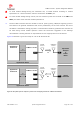
Table Of Contents
- Contents
- 1 System description
- 1.1 Overview
- 1.2 Architecture
- 1.3 Pin-out
- 1.4 Operating modes
- 1.5 Supply interfaces
- 1.5.1 Module supply input (VCC)
- 1.5.1.1 VCC supply requirements
- 1.5.1.2 VCC current consumption in 2G connected mode
- 1.5.1.3 VCC current consumption in 3G connected mode
- 1.5.1.4 VCC current consumption in LTE connected mode
- 1.5.1.5 VCC current consumption in cyclic low power idle mode / active mode
- 1.5.1.6 VCC current consumption in fixed active mode
- 1.5.2 Generic digital interfaces supply output (V_INT)
- 1.5.1 Module supply input (VCC)
- 1.6 System function interfaces
- 1.7 Antenna interfaces
- 1.8 SIM interfaces
- 1.9 Data communication interfaces
- 1.10 eMMC interface
- 1.11 Digital Audio interfaces
- 1.12 ADC interfaces
- 1.13 General Purpose Input/Output
- 1.14 Reserved pins (RSVD)
- 1.15 System features
- 1.15.1 Network indication
- 1.15.2 Jamming detection
- 1.15.3 IP modes of operation
- 1.15.4 Dual stack IPv4 and IPv6
- 1.15.5 Embedded TCP/IP and UDP/IP
- 1.15.6 Embedded FTP and FTPS
- 1.15.7 Embedded HTTP and HTTPS
- 1.15.8 SSL and TLS
- 1.15.9 Firmware update Over AT (FOAT)
- 1.15.10 Firmware update Over The Air (FOTA)
- 1.15.11 Power Saving
- 2 Design-in
- 2.1 Overview
- 2.2 Supply interfaces
- 2.2.1 Module supply (VCC)
- 2.2.1.1 General guidelines for VCC supply circuit selection and design
- 2.2.1.2 Guidelines for VCC supply circuit design using a switching regulator
- 2.2.1.3 Guidelines for VCC supply circuit design using a LDO linear regulator
- 2.2.1.4 Guidelines for VCC supply circuit design using a rechargeable battery
- 2.2.1.5 Guidelines for VCC supply circuit design using a primary battery
- 2.2.1.6 Additional guidelines for VCC supply circuit design
- 2.2.1.7 Guidelines for the external battery charging circuit
- 2.2.1.8 Guidelines for external charging and power path management circuit
- 2.2.1.9 Guidelines for removing VCC supply
- 2.2.1.10 Guidelines for VCC supply layout design
- 2.2.1.11 Guidelines for grounding layout design
- 2.2.2 Generic digital interfaces supply output (V_INT)
- 2.2.1 Module supply (VCC)
- 2.3 System functions interfaces
- 2.4 Antenna interface
- 2.5 SIM interfaces
- 2.6 Data communication interfaces
- 2.7 eMMC interface
- 2.8 Digital Audio interface
- 2.9 ADC interfaces
- 2.10 General Purpose Input/Output
- 2.11 Reserved pins (RSVD)
- 2.12 Module placement
- 2.13 Module footprint and paste mask
- 2.14 Thermal guidelines
- 2.15 Design-in checklist
- 3 Handling and soldering
- 4 Approvals
- 5 Product testing
- 6 FCC Notes
- Appendix
- Glossary
- Related documents
- Revision history
- Contact

TOBY-L3 series - System Integration Manual
TSD-19090601 - R13 System Integration Manual Page 136 of 143
6 FCC Notes
1. This module is limited to OEM installation ONLY.
2. This module is limited to installation in mobile or fixed applications, according to Part 2.1091(b).
3. The separate approval is required for all other operating configurations, including portable configurations
with respect to Part 2.1093 and different antenna configurations
4. For FCC Part 15.31 (h) and (k): The host manufacturer is responsible for additional testing to verify
compliance as a composite system. When testing the host device for compliance with Part 15 Subpart B,
the host manufacturer is required to show compliance with Part 15 Subpart B while the transmitter module(s)
are installed and operating. The modules should be transmitting and the evaluation should confirm that
the module's intentional emissions are compliant (i.e. fundamental and out of band emissions). The host
manufacturer must verify that there are no additional unintentional emissions other than what is permitted
in Part 15 Subpart B or emissions are complaint with the transmitter(s) rule(s). The Grantee will provide
guidance to the host manufacturer for Part 15 B requirements if needed.
End Product labeling
When the module is installed in the host device, the FCC ID label must be visible through a window on the
final device or it must be visible when an access panel, door or cover is easily re-moved. If not, a second
label must be placed on the outside of the final device that contains the following text:
“Contains FCC ID: 2A3Z6TOBYL3404 ”
The FCC ID can be used only when all FCC compliance requirements are met.
In the event that these conditions cannot be met (for example certain laptop configurations or co-location
with another transmitter), then the FCC authorization is no longer considered valid and the FCC ID cannot
be used on the final product. In these circumstances, the OEM integrator will be responsible for re-
evaluating the end product (including the transmitter) and obtaining a separate FCC authorization.
Manual Information to the End User
The OEM integrator has to be aware not to provide information to the end user regarding how to install
or remove this RF module in the user’s manual of the end product which integrates this module. The end
user manual shall include all required regulatory information/warning as show in this manual.
Federal Communication Commission Interference Statement
This device complies with Part 15 of the FCC Rules. Operation is subject to the following two conditions:
(1) This device may not cause harmful interference, and (2) this device must accept any interference received,
including interference that may cause undesired operation. This equipment has been tested and found to
comply with the limits for a Class B digital device, pursuant to Part 15 of the FCC Rules. These limits are