
Integration Manual


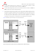
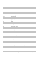
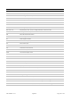
Table Of Contents
- Contents
- 1 System description
- 1.1 Overview
- 1.2 Architecture
- 1.3 Pin-out
- 1.4 Operating modes
- 1.5 Supply interfaces
- 1.5.1 Module supply input (VCC)
- 1.5.1.1 VCC supply requirements
- 1.5.1.2 VCC current consumption in 2G connected mode
- 1.5.1.3 VCC current consumption in 3G connected mode
- 1.5.1.4 VCC current consumption in LTE connected mode
- 1.5.1.5 VCC current consumption in cyclic low power idle mode / active mode
- 1.5.1.6 VCC current consumption in fixed active mode
- 1.5.2 Generic digital interfaces supply output (V_INT)
- 1.5.1 Module supply input (VCC)
- 1.6 System function interfaces
- 1.7 Antenna interfaces
- 1.8 SIM interfaces
- 1.9 Data communication interfaces
- 1.10 eMMC interface
- 1.11 Digital Audio interfaces
- 1.12 ADC interfaces
- 1.13 General Purpose Input/Output
- 1.14 Reserved pins (RSVD)
- 1.15 System features
- 1.15.1 Network indication
- 1.15.2 Jamming detection
- 1.15.3 IP modes of operation
- 1.15.4 Dual stack IPv4 and IPv6
- 1.15.5 Embedded TCP/IP and UDP/IP
- 1.15.6 Embedded FTP and FTPS
- 1.15.7 Embedded HTTP and HTTPS
- 1.15.8 SSL and TLS
- 1.15.9 Firmware update Over AT (FOAT)
- 1.15.10 Firmware update Over The Air (FOTA)
- 1.15.11 Power Saving
- 2 Design-in
- 2.1 Overview
- 2.2 Supply interfaces
- 2.2.1 Module supply (VCC)
- 2.2.1.1 General guidelines for VCC supply circuit selection and design
- 2.2.1.2 Guidelines for VCC supply circuit design using a switching regulator
- 2.2.1.3 Guidelines for VCC supply circuit design using a LDO linear regulator
- 2.2.1.4 Guidelines for VCC supply circuit design using a rechargeable battery
- 2.2.1.5 Guidelines for VCC supply circuit design using a primary battery
- 2.2.1.6 Additional guidelines for VCC supply circuit design
- 2.2.1.7 Guidelines for the external battery charging circuit
- 2.2.1.8 Guidelines for external charging and power path management circuit
- 2.2.1.9 Guidelines for removing VCC supply
- 2.2.1.10 Guidelines for VCC supply layout design
- 2.2.1.11 Guidelines for grounding layout design
- 2.2.2 Generic digital interfaces supply output (V_INT)
- 2.2.1 Module supply (VCC)
- 2.3 System functions interfaces
- 2.4 Antenna interface
- 2.5 SIM interfaces
- 2.6 Data communication interfaces
- 2.7 eMMC interface
- 2.8 Digital Audio interface
- 2.9 ADC interfaces
- 2.10 General Purpose Input/Output
- 2.11 Reserved pins (RSVD)
- 2.12 Module placement
- 2.13 Module footprint and paste mask
- 2.14 Thermal guidelines
- 2.15 Design-in checklist
- 3 Handling and soldering
- 4 Approvals
- 5 Product testing
- 6 FCC Notes
- Appendix
- Glossary
- Related documents
- Revision history
- Contact

TOBY-L3 series - System Integration Manual
TSD-19090601 - R13 System Integration Manual Page 135 of 143
⚠ To avoid module damage during the transmitter test, a suitable antenna according to module
specifications or a 50 termination must be connected to the ANT1 port.
⚠ To avoid module damage during receiver, test the maximum power level received at the ANT1 and
ANT2 ports which must meet the module specifications.
☞ The AT+UTEST command sets the module to emit RF power ignoring LTE/3G/2G signaling protocol.
This emission can generate interference that can be prohibited by law in some countries. The use of
this feature is intended for testing purposes in controlled environments by qualified users and must not
be used during normal module operation. Follow the instructions suggested in the Tashang’s
documentation. Tashang assumes no responsibilities for the inappropriate use of this feature.
Figure 62 illustrates a typical test setup for such an RF functional test.
Application Board
TOBY-L3 series
ANT1
Application
Processor
AT
commands
Cellular
antenna
Spectrum
Analyzer
or
Power
Meter
IN
Wideband
antenna
TX
Application Board
TOBY-L3 series
ANT1
Application
Processor
AT
commands
Cellular
antennas
Signal
Generator
OUT
Wideband
antenna
RX
ANT2
Figure 62: Setup with spectrum analyzer or power meter and signal generator for radiated measurements