
Integration Manual


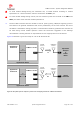
Table Of Contents
- Contents
- 1 System description
- 1.1 Overview
- 1.2 Architecture
- 1.3 Pin-out
- 1.4 Operating modes
- 1.5 Supply interfaces
- 1.5.1 Module supply input (VCC)
- 1.5.1.1 VCC supply requirements
- 1.5.1.2 VCC current consumption in 2G connected mode
- 1.5.1.3 VCC current consumption in 3G connected mode
- 1.5.1.4 VCC current consumption in LTE connected mode
- 1.5.1.5 VCC current consumption in cyclic low power idle mode / active mode
- 1.5.1.6 VCC current consumption in fixed active mode
- 1.5.2 Generic digital interfaces supply output (V_INT)
- 1.5.1 Module supply input (VCC)
- 1.6 System function interfaces
- 1.7 Antenna interfaces
- 1.8 SIM interfaces
- 1.9 Data communication interfaces
- 1.10 eMMC interface
- 1.11 Digital Audio interfaces
- 1.12 ADC interfaces
- 1.13 General Purpose Input/Output
- 1.14 Reserved pins (RSVD)
- 1.15 System features
- 1.15.1 Network indication
- 1.15.2 Jamming detection
- 1.15.3 IP modes of operation
- 1.15.4 Dual stack IPv4 and IPv6
- 1.15.5 Embedded TCP/IP and UDP/IP
- 1.15.6 Embedded FTP and FTPS
- 1.15.7 Embedded HTTP and HTTPS
- 1.15.8 SSL and TLS
- 1.15.9 Firmware update Over AT (FOAT)
- 1.15.10 Firmware update Over The Air (FOTA)
- 1.15.11 Power Saving
- 2 Design-in
- 2.1 Overview
- 2.2 Supply interfaces
- 2.2.1 Module supply (VCC)
- 2.2.1.1 General guidelines for VCC supply circuit selection and design
- 2.2.1.2 Guidelines for VCC supply circuit design using a switching regulator
- 2.2.1.3 Guidelines for VCC supply circuit design using a LDO linear regulator
- 2.2.1.4 Guidelines for VCC supply circuit design using a rechargeable battery
- 2.2.1.5 Guidelines for VCC supply circuit design using a primary battery
- 2.2.1.6 Additional guidelines for VCC supply circuit design
- 2.2.1.7 Guidelines for the external battery charging circuit
- 2.2.1.8 Guidelines for external charging and power path management circuit
- 2.2.1.9 Guidelines for removing VCC supply
- 2.2.1.10 Guidelines for VCC supply layout design
- 2.2.1.11 Guidelines for grounding layout design
- 2.2.2 Generic digital interfaces supply output (V_INT)
- 2.2.1 Module supply (VCC)
- 2.3 System functions interfaces
- 2.4 Antenna interface
- 2.5 SIM interfaces
- 2.6 Data communication interfaces
- 2.7 eMMC interface
- 2.8 Digital Audio interface
- 2.9 ADC interfaces
- 2.10 General Purpose Input/Output
- 2.11 Reserved pins (RSVD)
- 2.12 Module placement
- 2.13 Module footprint and paste mask
- 2.14 Thermal guidelines
- 2.15 Design-in checklist
- 3 Handling and soldering
- 4 Approvals
- 5 Product testing
- 6 FCC Notes
- Appendix
- Glossary
- Related documents
- Revision history
- Contact

TOBY-L3 series - System Integration Manual
TSD-19090601 - R13 System Integration Manual Page 134 of 143
5.2 Test parameters for OEM manufacturers
Because of the testing performed by Tashang (with 100% coverage), an OEM manufacturer does not need
to repeat firmware tests or measurements of the module RF performance or tests over digital interface in
their production test.
However, an OEM manufacturer should focus on:
Module assembly on the device; it should be verified that:
o Soldering and handling processes did not damage the module components
o All module pins are well soldered on the device board
o There are no short circuits between pins
Component assembly on the device; it should be verified that:
o Communications with the external host controller can be established
o The interfaces between the module and external devices are working
o Overall RF performance test of the device including the antenna
Dedicated tests can be implemented to check the device. For example, AT commands can be used to
perform functional tests on the modules’ interfaces (for more details see the TOBY-L3 series AT Commands
Manual [2]), in details:
Digital interfaces can be checked using the +UTEST=10 AT command
RF interfaces can be checked using the +UTEST AT command (see the following section 5.2.1)
5.2.1 RF functional tests
The overall RF functional test of the OEM device integrating the cellular module, including the antenna(s),
can be performed in the OEM production line with basic instruments such as a spectrum analyzer (or an
RF power meter) and a signal generator with the assistance of the AT+UTEST command over the AT
command user interface.
The +UTEST AT command provides a simple interface to set the module to Rx or Tx test modes ignoring
the LTE/3G/2G signaling protocol (for more details see the TOBY-L3 series AT Commands Manual [2]). The
command can set the module into:
transmitting mode in a specified channel and power level
receiving mode in a specified channel to returns the measured power level in all supported bands
This feature allows the measurement of the transmitter and receiver power levels to check component
assembly related to the module antenna interface and to check other device interfaces on which RF
performance depends.