
Integration Manual


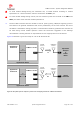
Table Of Contents
- Contents
- 1 System description
- 1.1 Overview
- 1.2 Architecture
- 1.3 Pin-out
- 1.4 Operating modes
- 1.5 Supply interfaces
- 1.5.1 Module supply input (VCC)
- 1.5.1.1 VCC supply requirements
- 1.5.1.2 VCC current consumption in 2G connected mode
- 1.5.1.3 VCC current consumption in 3G connected mode
- 1.5.1.4 VCC current consumption in LTE connected mode
- 1.5.1.5 VCC current consumption in cyclic low power idle mode / active mode
- 1.5.1.6 VCC current consumption in fixed active mode
- 1.5.2 Generic digital interfaces supply output (V_INT)
- 1.5.1 Module supply input (VCC)
- 1.6 System function interfaces
- 1.7 Antenna interfaces
- 1.8 SIM interfaces
- 1.9 Data communication interfaces
- 1.10 eMMC interface
- 1.11 Digital Audio interfaces
- 1.12 ADC interfaces
- 1.13 General Purpose Input/Output
- 1.14 Reserved pins (RSVD)
- 1.15 System features
- 1.15.1 Network indication
- 1.15.2 Jamming detection
- 1.15.3 IP modes of operation
- 1.15.4 Dual stack IPv4 and IPv6
- 1.15.5 Embedded TCP/IP and UDP/IP
- 1.15.6 Embedded FTP and FTPS
- 1.15.7 Embedded HTTP and HTTPS
- 1.15.8 SSL and TLS
- 1.15.9 Firmware update Over AT (FOAT)
- 1.15.10 Firmware update Over The Air (FOTA)
- 1.15.11 Power Saving
- 2 Design-in
- 2.1 Overview
- 2.2 Supply interfaces
- 2.2.1 Module supply (VCC)
- 2.2.1.1 General guidelines for VCC supply circuit selection and design
- 2.2.1.2 Guidelines for VCC supply circuit design using a switching regulator
- 2.2.1.3 Guidelines for VCC supply circuit design using a LDO linear regulator
- 2.2.1.4 Guidelines for VCC supply circuit design using a rechargeable battery
- 2.2.1.5 Guidelines for VCC supply circuit design using a primary battery
- 2.2.1.6 Additional guidelines for VCC supply circuit design
- 2.2.1.7 Guidelines for the external battery charging circuit
- 2.2.1.8 Guidelines for external charging and power path management circuit
- 2.2.1.9 Guidelines for removing VCC supply
- 2.2.1.10 Guidelines for VCC supply layout design
- 2.2.1.11 Guidelines for grounding layout design
- 2.2.2 Generic digital interfaces supply output (V_INT)
- 2.2.1 Module supply (VCC)
- 2.3 System functions interfaces
- 2.4 Antenna interface
- 2.5 SIM interfaces
- 2.6 Data communication interfaces
- 2.7 eMMC interface
- 2.8 Digital Audio interface
- 2.9 ADC interfaces
- 2.10 General Purpose Input/Output
- 2.11 Reserved pins (RSVD)
- 2.12 Module placement
- 2.13 Module footprint and paste mask
- 2.14 Thermal guidelines
- 2.15 Design-in checklist
- 3 Handling and soldering
- 4 Approvals
- 5 Product testing
- 6 FCC Notes
- Appendix
- Glossary
- Related documents
- Revision history
- Contact

TOBY-L3 series - System Integration Manual
TSD-19090601 - R13 System Integration Manual Page 131 of 143
4 Approvals
☞ For the complete list and specific details regarding the certification schemes approvals, see the TOBY-
L3 series Data Sheet [1], or contact the Tashang office or sales representative nearest you.
4.1 Product certification approval overview
Product certification approval is the process of certifying that a product has passed all tests and criteria
required by specifications, typically called “certification schemes” that can be divided into three distinct
categories:
Regulatory certification
o Country specific approval required by local government in most regions and countries, such as:
CE (Conformité Européenne) marking for the European Union
FCC (Federal Communications Commission) approval for the United States
Conformance certification
o Telecom industry specific approval verifying interoperability between devices and networks:
GCF (Global Certification Forum), a partnership between mainly European manufacturers and
network operators to ensure and verify global devices and networks interoperability
PTCRB (PCS Type Certification Review Board), created by United States network operators to
ensure and verify interoperability between devices and North America networks
Even using a module already approved under all major certification schemes, the application device
integrating the module must be approved under all the certification schemes required by the specific
application device to be deployed into the market. The required certification scheme approvals and relative
testing specifications differ depending on the country or the region where the device integrating the module
is intended to be deployed, on the relative vertical market of the device, on type, features and functionalities
of the whole application device, and on the network operators where the device is intended to operate.
☞ Check the appropriate applicability of the TOBY-L3 series module’s approvals while starting the
certification process of the device integrating the module: the re-use of the Tashang cellular module’s
approval can significantly reduce the cost and time-to-market of the application device certification.
☞ The certification of the application device that integrates a TOBY-L3 series module and the compliance
of the application device with all the applicable certification schemes, directives and standards are the
sole responsibility of the application device manufacturer.
TOBY-L3 series modules are certified according to all the supported capabilities, functions and options
stated in the Protocol Implementation Conformance Statement document (PICS) of the module. The PICS,
according to 3GPP TS 51.010-2 [11], 3GPP TS 34.121-2 [12], 3GPP TS 36.521-2 [14] and 3GPP TS 36.523-2