
Integration Manual
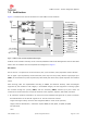
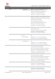


Table Of Contents
- Contents
- 1 System description
- 1.1 Overview
- 1.2 Architecture
- 1.3 Pin-out
- 1.4 Operating modes
- 1.5 Supply interfaces
- 1.5.1 Module supply input (VCC)
- 1.5.1.1 VCC supply requirements
- 1.5.1.2 VCC current consumption in 2G connected mode
- 1.5.1.3 VCC current consumption in 3G connected mode
- 1.5.1.4 VCC current consumption in LTE connected mode
- 1.5.1.5 VCC current consumption in cyclic low power idle mode / active mode
- 1.5.1.6 VCC current consumption in fixed active mode
- 1.5.2 Generic digital interfaces supply output (V_INT)
- 1.5.1 Module supply input (VCC)
- 1.6 System function interfaces
- 1.7 Antenna interfaces
- 1.8 SIM interfaces
- 1.9 Data communication interfaces
- 1.10 eMMC interface
- 1.11 Digital Audio interfaces
- 1.12 ADC interfaces
- 1.13 General Purpose Input/Output
- 1.14 Reserved pins (RSVD)
- 1.15 System features
- 1.15.1 Network indication
- 1.15.2 Jamming detection
- 1.15.3 IP modes of operation
- 1.15.4 Dual stack IPv4 and IPv6
- 1.15.5 Embedded TCP/IP and UDP/IP
- 1.15.6 Embedded FTP and FTPS
- 1.15.7 Embedded HTTP and HTTPS
- 1.15.8 SSL and TLS
- 1.15.9 Firmware update Over AT (FOAT)
- 1.15.10 Firmware update Over The Air (FOTA)
- 1.15.11 Power Saving
- 2 Design-in
- 2.1 Overview
- 2.2 Supply interfaces
- 2.2.1 Module supply (VCC)
- 2.2.1.1 General guidelines for VCC supply circuit selection and design
- 2.2.1.2 Guidelines for VCC supply circuit design using a switching regulator
- 2.2.1.3 Guidelines for VCC supply circuit design using a LDO linear regulator
- 2.2.1.4 Guidelines for VCC supply circuit design using a rechargeable battery
- 2.2.1.5 Guidelines for VCC supply circuit design using a primary battery
- 2.2.1.6 Additional guidelines for VCC supply circuit design
- 2.2.1.7 Guidelines for the external battery charging circuit
- 2.2.1.8 Guidelines for external charging and power path management circuit
- 2.2.1.9 Guidelines for removing VCC supply
- 2.2.1.10 Guidelines for VCC supply layout design
- 2.2.1.11 Guidelines for grounding layout design
- 2.2.2 Generic digital interfaces supply output (V_INT)
- 2.2.1 Module supply (VCC)
- 2.3 System functions interfaces
- 2.4 Antenna interface
- 2.5 SIM interfaces
- 2.6 Data communication interfaces
- 2.7 eMMC interface
- 2.8 Digital Audio interface
- 2.9 ADC interfaces
- 2.10 General Purpose Input/Output
- 2.11 Reserved pins (RSVD)
- 2.12 Module placement
- 2.13 Module footprint and paste mask
- 2.14 Thermal guidelines
- 2.15 Design-in checklist
- 3 Handling and soldering
- 4 Approvals
- 5 Product testing
- 6 FCC Notes
- Appendix
- Glossary
- Related documents
- Revision history
- Contact

TOBY-L3 series - System Integration Manual
TSD-19090601 - R13 System Integration Manual Page 13 of 143
Power Amplifiers (PA) amplify the Tx signal modulated by the RF transceiver
RF switches connect the primary (ANT1) and secondary (ANT2) antenna ports to the suitable Tx / Rx
path
SAW duplexers and band pass filters separate the Tx and Rx signal paths and provide RF filtering
19.2 MHz temperature-controlled crystal oscillator (TCXO) generates the clock reference in active mode
or connected mode.
Baseband and power management section
The Baseband and Power Management section is composed of the following main elements:
A mixed signal ASIC, which integrates
o Microprocessor for control functions
o DSP core for cellular Layer 1 and digital processing of Rx and Tx signal paths
o Memory interface controller
o Dedicated peripheral blocks for control of the USB, SIM and generic digital interfaces
o Interfaces to the RF transceiver ASIC
Memory system, which includes NAND flash and LPDDR2 RAM
Voltage regulators to derive all the subsystem supply voltages from the module supply input VCC
Voltage sources for external use: V_INT, V_SIM, V_ETH, V_MMC
Hardware power on
Hardware reset
Low power idle mode support
1.3 Pin-out
Table 4 lists the pin-out of the TOBY-L3 series modules, with pins grouped by function.
Function
Pin Name
Pin No
I/O
Description
Remarks
Power
VCC
70,71,72
I
Module supply input
VCC supply circuit affects the RF performance and
compliance of the device integrating the module with
applicable required certification schemes.
See section 1.5.1 for functional description / requirements.
See section 2.2.1 for external circuit design-in.
GND
2, 30, 32, 44, 46,
69, 73, 74, 76, 78,
79, 80, 82, 83, 85,
86, 88-90, 92-152,
209, 219, 226,
229, 232, 235,
238, 241
N/A
Ground
GND pins are internally connected each other.
External ground connection affects the RF and thermal
performance of the device.
See section 1.5.1for functional description.
See section 2.2.1 for external circuit design-in.