
Integration Manual
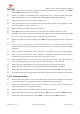


Table Of Contents
- Contents
- 1 System description
- 1.1 Overview
- 1.2 Architecture
- 1.3 Pin-out
- 1.4 Operating modes
- 1.5 Supply interfaces
- 1.5.1 Module supply input (VCC)
- 1.5.1.1 VCC supply requirements
- 1.5.1.2 VCC current consumption in 2G connected mode
- 1.5.1.3 VCC current consumption in 3G connected mode
- 1.5.1.4 VCC current consumption in LTE connected mode
- 1.5.1.5 VCC current consumption in cyclic low power idle mode / active mode
- 1.5.1.6 VCC current consumption in fixed active mode
- 1.5.2 Generic digital interfaces supply output (V_INT)
- 1.5.1 Module supply input (VCC)
- 1.6 System function interfaces
- 1.7 Antenna interfaces
- 1.8 SIM interfaces
- 1.9 Data communication interfaces
- 1.10 eMMC interface
- 1.11 Digital Audio interfaces
- 1.12 ADC interfaces
- 1.13 General Purpose Input/Output
- 1.14 Reserved pins (RSVD)
- 1.15 System features
- 1.15.1 Network indication
- 1.15.2 Jamming detection
- 1.15.3 IP modes of operation
- 1.15.4 Dual stack IPv4 and IPv6
- 1.15.5 Embedded TCP/IP and UDP/IP
- 1.15.6 Embedded FTP and FTPS
- 1.15.7 Embedded HTTP and HTTPS
- 1.15.8 SSL and TLS
- 1.15.9 Firmware update Over AT (FOAT)
- 1.15.10 Firmware update Over The Air (FOTA)
- 1.15.11 Power Saving
- 2 Design-in
- 2.1 Overview
- 2.2 Supply interfaces
- 2.2.1 Module supply (VCC)
- 2.2.1.1 General guidelines for VCC supply circuit selection and design
- 2.2.1.2 Guidelines for VCC supply circuit design using a switching regulator
- 2.2.1.3 Guidelines for VCC supply circuit design using a LDO linear regulator
- 2.2.1.4 Guidelines for VCC supply circuit design using a rechargeable battery
- 2.2.1.5 Guidelines for VCC supply circuit design using a primary battery
- 2.2.1.6 Additional guidelines for VCC supply circuit design
- 2.2.1.7 Guidelines for the external battery charging circuit
- 2.2.1.8 Guidelines for external charging and power path management circuit
- 2.2.1.9 Guidelines for removing VCC supply
- 2.2.1.10 Guidelines for VCC supply layout design
- 2.2.1.11 Guidelines for grounding layout design
- 2.2.2 Generic digital interfaces supply output (V_INT)
- 2.2.1 Module supply (VCC)
- 2.3 System functions interfaces
- 2.4 Antenna interface
- 2.5 SIM interfaces
- 2.6 Data communication interfaces
- 2.7 eMMC interface
- 2.8 Digital Audio interface
- 2.9 ADC interfaces
- 2.10 General Purpose Input/Output
- 2.11 Reserved pins (RSVD)
- 2.12 Module placement
- 2.13 Module footprint and paste mask
- 2.14 Thermal guidelines
- 2.15 Design-in checklist
- 3 Handling and soldering
- 4 Approvals
- 5 Product testing
- 6 FCC Notes
- Appendix
- Glossary
- Related documents
- Revision history
- Contact

TOBY-L3 series - System Integration Manual
TSD-19090601 - R13 System Integration Manual Page 128 of 143
Preheat Heating Cooling
[°C] Peak Temp. 245°C [°C]
250 250
Liquidus Temperature
217 217
200 200
40 - 60 s
End Temp.
max 4°C/s
150 - 200°C
150 150
max 3°C/s
60 - 120 s
100 Typical Leadfree 100
Soldering Profile
50 50
Elapsed time [s]
Figure 60: Recommended soldering profile
☞ The modules must not be soldered with a damp heat process.
3.3.3 Optical inspection
After soldering the module, inspect it optically to verify that it is properly aligned and centered.
3.3.4 Cleaning
Cleaning the modules is not recommended. Residues underneath the modules cannot be easily removed
with a washing process.
Cleaning with water will lead to capillary effects where water is absorbed in the gap between the
baseboard and the module. The combination of residues of soldering flux and encapsulated water leads
to short circuits or resistor-like interconnections between neighboring pads. Water will also damage the
sticker and the ink-jet printed text.
Cleaning with alcohol or other organic solvents can result in soldering flux residues flooding into the
two housings, areas that are not accessible for post-wash inspections. The solvent will also damage the
sticker and the ink-jet printed text.
Ultrasonic cleaning will permanently damage the module, in particular the quartz oscillators.
For best results, use a "no clean" soldering paste and eliminate the cleaning step after the soldering.
3.3.5 Repeated reflow soldering
Repeated reflow soldering processes and soldering the module upside down are not recommended.
Boards with components on both sides may require two reflow cycles. In this case, the module should
always be placed on the side of the board that is submitted into the last reflow cycle. The reason for this