
Integration Manual
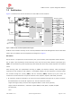


Table Of Contents
- Contents
- 1 System description
- 1.1 Overview
- 1.2 Architecture
- 1.3 Pin-out
- 1.4 Operating modes
- 1.5 Supply interfaces
- 1.5.1 Module supply input (VCC)
- 1.5.1.1 VCC supply requirements
- 1.5.1.2 VCC current consumption in 2G connected mode
- 1.5.1.3 VCC current consumption in 3G connected mode
- 1.5.1.4 VCC current consumption in LTE connected mode
- 1.5.1.5 VCC current consumption in cyclic low power idle mode / active mode
- 1.5.1.6 VCC current consumption in fixed active mode
- 1.5.2 Generic digital interfaces supply output (V_INT)
- 1.5.1 Module supply input (VCC)
- 1.6 System function interfaces
- 1.7 Antenna interfaces
- 1.8 SIM interfaces
- 1.9 Data communication interfaces
- 1.10 eMMC interface
- 1.11 Digital Audio interfaces
- 1.12 ADC interfaces
- 1.13 General Purpose Input/Output
- 1.14 Reserved pins (RSVD)
- 1.15 System features
- 1.15.1 Network indication
- 1.15.2 Jamming detection
- 1.15.3 IP modes of operation
- 1.15.4 Dual stack IPv4 and IPv6
- 1.15.5 Embedded TCP/IP and UDP/IP
- 1.15.6 Embedded FTP and FTPS
- 1.15.7 Embedded HTTP and HTTPS
- 1.15.8 SSL and TLS
- 1.15.9 Firmware update Over AT (FOAT)
- 1.15.10 Firmware update Over The Air (FOTA)
- 1.15.11 Power Saving
- 2 Design-in
- 2.1 Overview
- 2.2 Supply interfaces
- 2.2.1 Module supply (VCC)
- 2.2.1.1 General guidelines for VCC supply circuit selection and design
- 2.2.1.2 Guidelines for VCC supply circuit design using a switching regulator
- 2.2.1.3 Guidelines for VCC supply circuit design using a LDO linear regulator
- 2.2.1.4 Guidelines for VCC supply circuit design using a rechargeable battery
- 2.2.1.5 Guidelines for VCC supply circuit design using a primary battery
- 2.2.1.6 Additional guidelines for VCC supply circuit design
- 2.2.1.7 Guidelines for the external battery charging circuit
- 2.2.1.8 Guidelines for external charging and power path management circuit
- 2.2.1.9 Guidelines for removing VCC supply
- 2.2.1.10 Guidelines for VCC supply layout design
- 2.2.1.11 Guidelines for grounding layout design
- 2.2.2 Generic digital interfaces supply output (V_INT)
- 2.2.1 Module supply (VCC)
- 2.3 System functions interfaces
- 2.4 Antenna interface
- 2.5 SIM interfaces
- 2.6 Data communication interfaces
- 2.7 eMMC interface
- 2.8 Digital Audio interface
- 2.9 ADC interfaces
- 2.10 General Purpose Input/Output
- 2.11 Reserved pins (RSVD)
- 2.12 Module placement
- 2.13 Module footprint and paste mask
- 2.14 Thermal guidelines
- 2.15 Design-in checklist
- 3 Handling and soldering
- 4 Approvals
- 5 Product testing
- 6 FCC Notes
- Appendix
- Glossary
- Related documents
- Revision history
- Contact

TOBY-L3 series - System Integration Manual
TSD-19090601 - R13 System Integration Manual Page 12 of 143
1.2 Architecture
Figure 1 summarizes the internal architecture of the TOBY-L3 series modules.
Cellular
Base-band
Processor
Memory
Power Management Unit
19.2 MHz
RF
Transceiver
V_INT (I/O)
VCC (Supply)
1 x SIM
USB 2.0
2 x ADC
Power on
External reset
2 x DDC (I
2
C)
SDIO
4 x UART
Antenna detection
Host Select
ANT2
Filter
s
Filters
Switch
ANT1
PAs
Filter
s
Filter
s
Duplexe
r
Filters
PAs
Filter
s
Filter
s
Duplexe
r
Filters
Switch
1 x SPI
SGMII
eMCC
Digital audio (I
2
S)
GPIOs
Figure 1: TOBY-L3 series modules simplified block diagram
TOBY-L3 series modules internally consist of the RF, Baseband and Power Management sections described
herein with more details than the simplified block diagrams of Figure 1.
RF section
The RF section is composed of an RF transceiver, PAs, crystal oscillator, filters, duplexers and RF switches.
The Tx signal is pre-amplified by the RF transceiver, then output to the primary antenna input/output port
(ANT1) of the module via power amplifier (PA), SAW band pass filters band, specific duplexer and antenna
switch.
Dual receiving paths are implemented according to MIMO, and Receiver Diversity radio technologies
supported by the modules as LTE category 4 and HSDPA category 24 User Equipment: incoming signals
are received through the primary (ANT1) and the secondary (ANT2) antenna input ports which are
connected to the RF transceiver via specific antenna switch, diplexer, duplexer, SAW band pass filters.
RF transceiver performs modulation, up-conversion of the baseband I/O signals for Tx, down-conversion
and demodulation of the dual RF signals for Rx. The RF transceiver contains:
Single chain high linearity receivers with integrated LNAs for multi-mode operation,
Highly linear RF demodulator / modulator capable GMSK, 8-PSK, QPSK, 16-QAM, 64-QAM
RF synthesizer,
VCO.