
Integration Manual

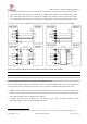
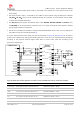
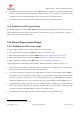


Table Of Contents
- Contents
- 1 System description
- 1.1 Overview
- 1.2 Architecture
- 1.3 Pin-out
- 1.4 Operating modes
- 1.5 Supply interfaces
- 1.5.1 Module supply input (VCC)
- 1.5.1.1 VCC supply requirements
- 1.5.1.2 VCC current consumption in 2G connected mode
- 1.5.1.3 VCC current consumption in 3G connected mode
- 1.5.1.4 VCC current consumption in LTE connected mode
- 1.5.1.5 VCC current consumption in cyclic low power idle mode / active mode
- 1.5.1.6 VCC current consumption in fixed active mode
- 1.5.2 Generic digital interfaces supply output (V_INT)
- 1.5.1 Module supply input (VCC)
- 1.6 System function interfaces
- 1.7 Antenna interfaces
- 1.8 SIM interfaces
- 1.9 Data communication interfaces
- 1.10 eMMC interface
- 1.11 Digital Audio interfaces
- 1.12 ADC interfaces
- 1.13 General Purpose Input/Output
- 1.14 Reserved pins (RSVD)
- 1.15 System features
- 1.15.1 Network indication
- 1.15.2 Jamming detection
- 1.15.3 IP modes of operation
- 1.15.4 Dual stack IPv4 and IPv6
- 1.15.5 Embedded TCP/IP and UDP/IP
- 1.15.6 Embedded FTP and FTPS
- 1.15.7 Embedded HTTP and HTTPS
- 1.15.8 SSL and TLS
- 1.15.9 Firmware update Over AT (FOAT)
- 1.15.10 Firmware update Over The Air (FOTA)
- 1.15.11 Power Saving
- 2 Design-in
- 2.1 Overview
- 2.2 Supply interfaces
- 2.2.1 Module supply (VCC)
- 2.2.1.1 General guidelines for VCC supply circuit selection and design
- 2.2.1.2 Guidelines for VCC supply circuit design using a switching regulator
- 2.2.1.3 Guidelines for VCC supply circuit design using a LDO linear regulator
- 2.2.1.4 Guidelines for VCC supply circuit design using a rechargeable battery
- 2.2.1.5 Guidelines for VCC supply circuit design using a primary battery
- 2.2.1.6 Additional guidelines for VCC supply circuit design
- 2.2.1.7 Guidelines for the external battery charging circuit
- 2.2.1.8 Guidelines for external charging and power path management circuit
- 2.2.1.9 Guidelines for removing VCC supply
- 2.2.1.10 Guidelines for VCC supply layout design
- 2.2.1.11 Guidelines for grounding layout design
- 2.2.2 Generic digital interfaces supply output (V_INT)
- 2.2.1 Module supply (VCC)
- 2.3 System functions interfaces
- 2.4 Antenna interface
- 2.5 SIM interfaces
- 2.6 Data communication interfaces
- 2.7 eMMC interface
- 2.8 Digital Audio interface
- 2.9 ADC interfaces
- 2.10 General Purpose Input/Output
- 2.11 Reserved pins (RSVD)
- 2.12 Module placement
- 2.13 Module footprint and paste mask
- 2.14 Thermal guidelines
- 2.15 Design-in checklist
- 3 Handling and soldering
- 4 Approvals
- 5 Product testing
- 6 FCC Notes
- Appendix
- Glossary
- Related documents
- Revision history
- Contact

TOBY-L3 series - System Integration Manual
TSD-19090601 - R13 System Integration Manual Page 119 of 143
2.13 Module footprint and paste mask
Figure 59 and Table 46 describe the suggested footprint (i.e. copper mask) and the paste mask (i.e. stencil)
layout for TOBY-L3 series modules, to be implemented on the application PCB.
The proposed land pattern layout (i.e. the footprint, the application board top-layer copper mask) reflects
the modules’ pads layout, with the pads on the application board designed as the LGA pads of the module.
I
A
D
F
K
M1
M1
M2
P2
B
G1 HJ
L N
M1
M1
M3
II OJJ J
E
P3
F
P1
H
O
M1
H
G2G2
G1
H
J
I
H
O
O
0.80
1.50
1.45
0.60
0.10
0.17
Copper
Past e
1.10
1.10
1.00
1.00
0.05
0.05
Past e
Copper
1.10
1.10
0.90
0.90
0.10
0.10
Past e
Copper
0.80
1.50
1.38
0.60
0.10
0.06
Past e
Copper
Figure 59: Suggested footprint and stencil design for TOBY-L3 modules, to be implemented on application PCB (top view)
Parameter
Value
Parameter
Value
Parameter
Value
Parameter
Value
A
35.6 mm
G1
1.10 mm
K
3.15 mm
N
2.10 mm
B
24.8 mm
G2
2.00 mm
L
7.15 mm
O
1.10 mm
D
2.40 mm
H
0.80 mm
M1
1.80 mm
P1
1.10 mm
E
2.25 mm
I
1.50 mm
M2
3.40 mm
P2
1.25 mm
F
1.45 mm
J
0.30 mm
M3
2.25 mm
P3
2.85 mm
Table 46: Suggested footprint design dimensions for TOBY-L3 series modules, to be implemented on application PCB
Non Solder resist Mask Defined pad type is recommended over Solder resist Mask Defined type, designing
the solder resist mask opening 50 µm larger per side than the corresponding copper pad.
The suggested paste mask (i.e. stencil) layout to mount the modules on the application PCB is also illustrated
in Figure 59. Different stencil apertures layout for any specific pad is recommended:
Green marked pads: Paste layout enlarged on the lateral side and reduced on other sides
Light-Green marked pads: Paste layout reduced circumferentially to Copper layout
Blue marked pads: Paste layout reduced circumferentially 0.05 mm to Copper layout