
Integration Manual
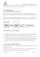

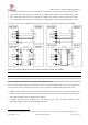
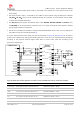


Table Of Contents
- Contents
- 1 System description
- 1.1 Overview
- 1.2 Architecture
- 1.3 Pin-out
- 1.4 Operating modes
- 1.5 Supply interfaces
- 1.5.1 Module supply input (VCC)
- 1.5.1.1 VCC supply requirements
- 1.5.1.2 VCC current consumption in 2G connected mode
- 1.5.1.3 VCC current consumption in 3G connected mode
- 1.5.1.4 VCC current consumption in LTE connected mode
- 1.5.1.5 VCC current consumption in cyclic low power idle mode / active mode
- 1.5.1.6 VCC current consumption in fixed active mode
- 1.5.2 Generic digital interfaces supply output (V_INT)
- 1.5.1 Module supply input (VCC)
- 1.6 System function interfaces
- 1.7 Antenna interfaces
- 1.8 SIM interfaces
- 1.9 Data communication interfaces
- 1.10 eMMC interface
- 1.11 Digital Audio interfaces
- 1.12 ADC interfaces
- 1.13 General Purpose Input/Output
- 1.14 Reserved pins (RSVD)
- 1.15 System features
- 1.15.1 Network indication
- 1.15.2 Jamming detection
- 1.15.3 IP modes of operation
- 1.15.4 Dual stack IPv4 and IPv6
- 1.15.5 Embedded TCP/IP and UDP/IP
- 1.15.6 Embedded FTP and FTPS
- 1.15.7 Embedded HTTP and HTTPS
- 1.15.8 SSL and TLS
- 1.15.9 Firmware update Over AT (FOAT)
- 1.15.10 Firmware update Over The Air (FOTA)
- 1.15.11 Power Saving
- 2 Design-in
- 2.1 Overview
- 2.2 Supply interfaces
- 2.2.1 Module supply (VCC)
- 2.2.1.1 General guidelines for VCC supply circuit selection and design
- 2.2.1.2 Guidelines for VCC supply circuit design using a switching regulator
- 2.2.1.3 Guidelines for VCC supply circuit design using a LDO linear regulator
- 2.2.1.4 Guidelines for VCC supply circuit design using a rechargeable battery
- 2.2.1.5 Guidelines for VCC supply circuit design using a primary battery
- 2.2.1.6 Additional guidelines for VCC supply circuit design
- 2.2.1.7 Guidelines for the external battery charging circuit
- 2.2.1.8 Guidelines for external charging and power path management circuit
- 2.2.1.9 Guidelines for removing VCC supply
- 2.2.1.10 Guidelines for VCC supply layout design
- 2.2.1.11 Guidelines for grounding layout design
- 2.2.2 Generic digital interfaces supply output (V_INT)
- 2.2.1 Module supply (VCC)
- 2.3 System functions interfaces
- 2.4 Antenna interface
- 2.5 SIM interfaces
- 2.6 Data communication interfaces
- 2.7 eMMC interface
- 2.8 Digital Audio interface
- 2.9 ADC interfaces
- 2.10 General Purpose Input/Output
- 2.11 Reserved pins (RSVD)
- 2.12 Module placement
- 2.13 Module footprint and paste mask
- 2.14 Thermal guidelines
- 2.15 Design-in checklist
- 3 Handling and soldering
- 4 Approvals
- 5 Product testing
- 6 FCC Notes
- Appendix
- Glossary
- Related documents
- Revision history
- Contact

TOBY-L3 series - System Integration Manual
TSD-19090601 - R13 System Integration Manual Page 116 of 143
R2,R3
2.2 k Resistor 0402 0.1% 62.5 mW
RN73R1ETP2201B25 - KOA
D1,D2
Low Capacitance ESD Protection
USB0002RP or USB0002DP – AVX
U1
LDO Linear Regulator 1.8 V 0.3 A
LT1962EMS8-1.8 - Linear Technology
U2
Audio Voice Codec
ALC5660 - Realtek
Table 45: Example of components for an ACL5660 audio voice codec application circuit
☞ Do not apply voltage to any PCM digital audio interface pins before the switch-on of the supply source
(V_INT), to avoid latch-up of circuits and allow a clean boot of the module.
☞ The ESD sensitivity rating of the I
2
S interface pins is 1 kV (Human Body Model according to JESD22-
A114). A higher protection level could be required if the lines are externally accessible and it can be
achieved by mounting a general purpose ESD protection (e.g. EPCOS CA05P4S14THSG varistor array)
close to the accessible points.
☞ If the PCM digital audio pins or the I2C pins (I2C_SDA1, I2C_SCL1) are not used, they can be left
unconnected on the application board.
2.8.2 Guidelines for digital audio layout design
I
2
S interface and clock output lines require the same considerations regarding electromagnetic interference
as any other high speed digital interface. Keep the traces short and avoid coupling with RF lines / parts or
sensitive analog inputs, since the signals can cause the radiation of some harmonics of the digital data
frequency.
2.9 ADC interfaces
☞ The ADC pins are not supported by the "0x" product feature versions.
2.9.1 Guidelines for ADC circuit design
TOBY-L3 series modules include Analog to Digital Converter inputs (ADC1, ADC2), which can be handled
by means of the dedicated open CPU API.
The ADC pins can be connected to external circuits for general purpose voltage measurements.
The voltage value at the ADC input must be within the range reported in the TOBY-L3 series Data Sheet [1].
If an external voltage divider is implemented to increase the measurement voltage range, check the input
resistance of the ADC inputs reported in the TOBY-L3 series Data Sheet [1]: if the equivalent of the external
circuit has a significant value as compared to the input resistance of the ADC inputs, this should be taken
into account and corrected to properly associate the ADC response to the voltage source value,
implementing an appropriate ADC calibration procedure.