
Integration Manual
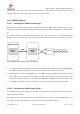

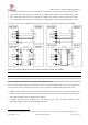
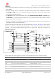


Table Of Contents
- Contents
- 1 System description
- 1.1 Overview
- 1.2 Architecture
- 1.3 Pin-out
- 1.4 Operating modes
- 1.5 Supply interfaces
- 1.5.1 Module supply input (VCC)
- 1.5.1.1 VCC supply requirements
- 1.5.1.2 VCC current consumption in 2G connected mode
- 1.5.1.3 VCC current consumption in 3G connected mode
- 1.5.1.4 VCC current consumption in LTE connected mode
- 1.5.1.5 VCC current consumption in cyclic low power idle mode / active mode
- 1.5.1.6 VCC current consumption in fixed active mode
- 1.5.2 Generic digital interfaces supply output (V_INT)
- 1.5.1 Module supply input (VCC)
- 1.6 System function interfaces
- 1.7 Antenna interfaces
- 1.8 SIM interfaces
- 1.9 Data communication interfaces
- 1.10 eMMC interface
- 1.11 Digital Audio interfaces
- 1.12 ADC interfaces
- 1.13 General Purpose Input/Output
- 1.14 Reserved pins (RSVD)
- 1.15 System features
- 1.15.1 Network indication
- 1.15.2 Jamming detection
- 1.15.3 IP modes of operation
- 1.15.4 Dual stack IPv4 and IPv6
- 1.15.5 Embedded TCP/IP and UDP/IP
- 1.15.6 Embedded FTP and FTPS
- 1.15.7 Embedded HTTP and HTTPS
- 1.15.8 SSL and TLS
- 1.15.9 Firmware update Over AT (FOAT)
- 1.15.10 Firmware update Over The Air (FOTA)
- 1.15.11 Power Saving
- 2 Design-in
- 2.1 Overview
- 2.2 Supply interfaces
- 2.2.1 Module supply (VCC)
- 2.2.1.1 General guidelines for VCC supply circuit selection and design
- 2.2.1.2 Guidelines for VCC supply circuit design using a switching regulator
- 2.2.1.3 Guidelines for VCC supply circuit design using a LDO linear regulator
- 2.2.1.4 Guidelines for VCC supply circuit design using a rechargeable battery
- 2.2.1.5 Guidelines for VCC supply circuit design using a primary battery
- 2.2.1.6 Additional guidelines for VCC supply circuit design
- 2.2.1.7 Guidelines for the external battery charging circuit
- 2.2.1.8 Guidelines for external charging and power path management circuit
- 2.2.1.9 Guidelines for removing VCC supply
- 2.2.1.10 Guidelines for VCC supply layout design
- 2.2.1.11 Guidelines for grounding layout design
- 2.2.2 Generic digital interfaces supply output (V_INT)
- 2.2.1 Module supply (VCC)
- 2.3 System functions interfaces
- 2.4 Antenna interface
- 2.5 SIM interfaces
- 2.6 Data communication interfaces
- 2.7 eMMC interface
- 2.8 Digital Audio interface
- 2.9 ADC interfaces
- 2.10 General Purpose Input/Output
- 2.11 Reserved pins (RSVD)
- 2.12 Module placement
- 2.13 Module footprint and paste mask
- 2.14 Thermal guidelines
- 2.15 Design-in checklist
- 3 Handling and soldering
- 4 Approvals
- 5 Product testing
- 6 FCC Notes
- Appendix
- Glossary
- Related documents
- Revision history
- Contact

TOBY-L3 series - System Integration Manual
TSD-19090601 - R13 System Integration Manual Page 113 of 143
2.8 Digital Audio interface
2.8.1 Guidelines for digital audio circuit design
I
2
S digital audio interfaces can be connected to external digital audio devices for voice applications.
Any external digital audio device compliant with the configuration of the digital audio interface of the
TOBY-L3 series cellular module can be used, given that the external digital audio device must provide:
The opposite role: slave or master role, as TOBY-L3 series modules may act as master or slave
The same mode and frame format: PCM / short synch mode or Normal I
2
S / long synch mode with
o data in 2’s complement notation, linear
o MSB transmitted first
o data word length = 16-bit (16 clock cycles)
o frame length = synch signal period:
17-bit or 18-bit in PCM / short alignment mode (16 + 1 or 16 + 2 clock cycles, with the Word
Alignment / Synchronization signal set high for 1 clock cycle or 2 clock cycles)
32-bit in Normal I
2
S mode / long alignment mode (16 x 2 clock cycles)
The same sample rate, i.e. synch signal frequency, <I2S_sample_rate> parameter:
o 8 kHz, 16 kHz, 48 kHz
The same serial clock frequency:
o 17 x <I2S_sample_rate> or 18 x <I2S_sample_rate> in PCM / short alignment mode, or
o 16 x 2 x <I2S_sample_rate> in Normal I
2
S mode / long alignment mode
Compatible voltage levels (1.80 V typ.), otherwise it is recommended to connect the 1.8 V digital audio
interface of the module to the external 3.0 V (or similar) digital audio device by means of appropriate
unidirectional voltage translators (e.g. TI SN74AVC4T774 or SN74AVC2T245, providing a partial power
down feature so that the digital audio device 3.0 V supply can be also ramped up before V_INT 1.8 V
supply), using the module V_INT output as 1.8 V supply for the voltage translators on the module side.
An appropriate specific application circuit must be implemented and configured according to the particular
external digital audio device or codec used and according to the application requirements.
Examples of manufacturers offering compatible audio codec parts are the following:
Maxim Integrated (as the MAX9860, MAX9867, MAX9880A audio codecs)
Texas Instruments / National Semiconductor
Cirrus Logic / Wolfson Microelectronics
Nuvoton Technology
Asahi Kasei Microdevices
Realtek Semiconductor
Figure 57 and Table 44 describe circuits for the digital audio interfaces, considering these scenarios: