
Integration Manual
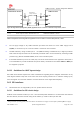

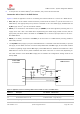


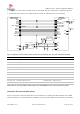
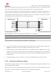
Table Of Contents
- Contents
- 1 System description
- 1.1 Overview
- 1.2 Architecture
- 1.3 Pin-out
- 1.4 Operating modes
- 1.5 Supply interfaces
- 1.5.1 Module supply input (VCC)
- 1.5.1.1 VCC supply requirements
- 1.5.1.2 VCC current consumption in 2G connected mode
- 1.5.1.3 VCC current consumption in 3G connected mode
- 1.5.1.4 VCC current consumption in LTE connected mode
- 1.5.1.5 VCC current consumption in cyclic low power idle mode / active mode
- 1.5.1.6 VCC current consumption in fixed active mode
- 1.5.2 Generic digital interfaces supply output (V_INT)
- 1.5.1 Module supply input (VCC)
- 1.6 System function interfaces
- 1.7 Antenna interfaces
- 1.8 SIM interfaces
- 1.9 Data communication interfaces
- 1.10 eMMC interface
- 1.11 Digital Audio interfaces
- 1.12 ADC interfaces
- 1.13 General Purpose Input/Output
- 1.14 Reserved pins (RSVD)
- 1.15 System features
- 1.15.1 Network indication
- 1.15.2 Jamming detection
- 1.15.3 IP modes of operation
- 1.15.4 Dual stack IPv4 and IPv6
- 1.15.5 Embedded TCP/IP and UDP/IP
- 1.15.6 Embedded FTP and FTPS
- 1.15.7 Embedded HTTP and HTTPS
- 1.15.8 SSL and TLS
- 1.15.9 Firmware update Over AT (FOAT)
- 1.15.10 Firmware update Over The Air (FOTA)
- 1.15.11 Power Saving
- 2 Design-in
- 2.1 Overview
- 2.2 Supply interfaces
- 2.2.1 Module supply (VCC)
- 2.2.1.1 General guidelines for VCC supply circuit selection and design
- 2.2.1.2 Guidelines for VCC supply circuit design using a switching regulator
- 2.2.1.3 Guidelines for VCC supply circuit design using a LDO linear regulator
- 2.2.1.4 Guidelines for VCC supply circuit design using a rechargeable battery
- 2.2.1.5 Guidelines for VCC supply circuit design using a primary battery
- 2.2.1.6 Additional guidelines for VCC supply circuit design
- 2.2.1.7 Guidelines for the external battery charging circuit
- 2.2.1.8 Guidelines for external charging and power path management circuit
- 2.2.1.9 Guidelines for removing VCC supply
- 2.2.1.10 Guidelines for VCC supply layout design
- 2.2.1.11 Guidelines for grounding layout design
- 2.2.2 Generic digital interfaces supply output (V_INT)
- 2.2.1 Module supply (VCC)
- 2.3 System functions interfaces
- 2.4 Antenna interface
- 2.5 SIM interfaces
- 2.6 Data communication interfaces
- 2.7 eMMC interface
- 2.8 Digital Audio interface
- 2.9 ADC interfaces
- 2.10 General Purpose Input/Output
- 2.11 Reserved pins (RSVD)
- 2.12 Module placement
- 2.13 Module footprint and paste mask
- 2.14 Thermal guidelines
- 2.15 Design-in checklist
- 3 Handling and soldering
- 4 Approvals
- 5 Product testing
- 6 FCC Notes
- Appendix
- Glossary
- Related documents
- Revision history
- Contact

TOBY-L3 series - System Integration Manual
TSD-19090601 - R13 System Integration Manual Page 106 of 143
R5
100 k Resistor 0402 5% 0.1 W
RC0402JR-07100KL - Yageo Phycomp
T1
P-Channel MOSFET Low On-Resistance
IRLML6401 - International Rectifier or NTZS3151P - ON
Semi
T2
NPN BJT Transistor
BC847 - Infineon
C1
100 nF Capacitor Ceramic X7R 0402 10% 16 V
GRM155R71C104KA01 - Murata
Table 40: Components for connecting TOBY-L3 series modules to u-blox 1.8 V GNSS devices using V_INT as supply
Connection with u-blox 3.0 V GNSS devices
Figure 53 shows an application circuit for connecting the cellular modules to a u-blox 3.0 V GNSS device:
As the SDA and SCL pins of the cellular module are not tolerant up to 3.0 V, the connection to the
related I
2
C pins of the u-blox 3.0 V GNSS device must be provided using a suitable I
2
C-bus Bidirectional
Voltage Translator with appropriate pull-up resistors (e.g. the TI TCA9406 additionally provides the partial
power down feature so that the GNSS 3.0 V supply can be ramped up before the V_INT 1.8 V cellular
supply).
GPIO2 pin is connected to the shutdown input pin (SHDNn) of the LDO regulators providing the 3.0 V
supply rail for the u-blox 3.0 V GNSS device implementing the “GNSS enable” function, with an
appropriate pull-down resistor mounted on the GPIO2 line to avoid an improper switch-on of the u-
blox GNSS device.
As the GPIO3 pin of the cellular module is not tolerant up to 3.0 V, the connection to the related pin of
the u-blox 3.0 V GNSS device must be provided using a suitable Unidirectional General Purpose Voltage
Translator (e.g. TI SN74LVC1T45, which additionally provides the partial power down feature so that the
3.0 V GNSS supply can be also ramped up before the V_INT 1.8 V rail).
The V_BCKP backup supply input pin of the GNSS device is connected to the external battery as in the
application circuit for a u-blox 1.8 V GNSS device.