
Integration Manual
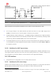


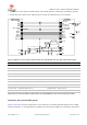
Table Of Contents
- Contents
- 1 System description
- 1.1 Overview
- 1.2 Architecture
- 1.3 Pin-out
- 1.4 Operating modes
- 1.5 Supply interfaces
- 1.5.1 Module supply input (VCC)
- 1.5.1.1 VCC supply requirements
- 1.5.1.2 VCC current consumption in 2G connected mode
- 1.5.1.3 VCC current consumption in 3G connected mode
- 1.5.1.4 VCC current consumption in LTE connected mode
- 1.5.1.5 VCC current consumption in cyclic low power idle mode / active mode
- 1.5.1.6 VCC current consumption in fixed active mode
- 1.5.2 Generic digital interfaces supply output (V_INT)
- 1.5.1 Module supply input (VCC)
- 1.6 System function interfaces
- 1.7 Antenna interfaces
- 1.8 SIM interfaces
- 1.9 Data communication interfaces
- 1.10 eMMC interface
- 1.11 Digital Audio interfaces
- 1.12 ADC interfaces
- 1.13 General Purpose Input/Output
- 1.14 Reserved pins (RSVD)
- 1.15 System features
- 1.15.1 Network indication
- 1.15.2 Jamming detection
- 1.15.3 IP modes of operation
- 1.15.4 Dual stack IPv4 and IPv6
- 1.15.5 Embedded TCP/IP and UDP/IP
- 1.15.6 Embedded FTP and FTPS
- 1.15.7 Embedded HTTP and HTTPS
- 1.15.8 SSL and TLS
- 1.15.9 Firmware update Over AT (FOAT)
- 1.15.10 Firmware update Over The Air (FOTA)
- 1.15.11 Power Saving
- 2 Design-in
- 2.1 Overview
- 2.2 Supply interfaces
- 2.2.1 Module supply (VCC)
- 2.2.1.1 General guidelines for VCC supply circuit selection and design
- 2.2.1.2 Guidelines for VCC supply circuit design using a switching regulator
- 2.2.1.3 Guidelines for VCC supply circuit design using a LDO linear regulator
- 2.2.1.4 Guidelines for VCC supply circuit design using a rechargeable battery
- 2.2.1.5 Guidelines for VCC supply circuit design using a primary battery
- 2.2.1.6 Additional guidelines for VCC supply circuit design
- 2.2.1.7 Guidelines for the external battery charging circuit
- 2.2.1.8 Guidelines for external charging and power path management circuit
- 2.2.1.9 Guidelines for removing VCC supply
- 2.2.1.10 Guidelines for VCC supply layout design
- 2.2.1.11 Guidelines for grounding layout design
- 2.2.2 Generic digital interfaces supply output (V_INT)
- 2.2.1 Module supply (VCC)
- 2.3 System functions interfaces
- 2.4 Antenna interface
- 2.5 SIM interfaces
- 2.6 Data communication interfaces
- 2.7 eMMC interface
- 2.8 Digital Audio interface
- 2.9 ADC interfaces
- 2.10 General Purpose Input/Output
- 2.11 Reserved pins (RSVD)
- 2.12 Module placement
- 2.13 Module footprint and paste mask
- 2.14 Thermal guidelines
- 2.15 Design-in checklist
- 3 Handling and soldering
- 4 Approvals
- 5 Product testing
- 6 FCC Notes
- Appendix
- Glossary
- Related documents
- Revision history
- Contact

TOBY-L3 series - System Integration Manual
TSD-19090601 - R13 System Integration Manual Page 104 of 143
☞ If the pins are not used as DDC (I
2
C) bus interface, they can be left unconnected.
Connection with u-blox 1.8 V GNSS devices
Figure 51 shows an application circuit for connecting the cellular modules to a u-blox 1.8 V GNSS device.
SDA / SCL pins of the cellular module are directly connected to the relative I
2
C pins of the u-blox 1.8 V
GNSS device, with appropriate pull-up resistors connected to the 1.8 V GNSS supply enabled after the
V_INT supply of the I
2
C pins of the cellular module.
GPIO2 pin is connected to the shutdown input pin (SHDNn) of the LDO regulators providing the 1.8 V
supply rail for the u-blox 1.8 V GNSS device implementing the “GNSS supply enable” function, with an
appropriate pull-down resistor mounted on the GPIO2 line to avoid an improper switch-on of the u-
blox GNSS device.
GPIO3 pin is directly connected to the TXD1 pin of the u-blox 1.8 V GNSS device providing “GNSS Tx
data ready” function.
The V_BCKP backup supply input pin of the GNSS device is connected to the external battery to provide
the supply for the GNSS real time clock and backup RAM when the VCC supply of the cellular module
is within its operating range and the VCC supply of the GNSS device is disabled. This enables the u-blox
GNSS device to recover from a power breakdown with either a hot start or a warm start (depending on
the actual duration of the GNSS VCC outage) and to maintain the configuration settings saved in the
backup RAM.
R1
IN
OUT
GND
GNSS LDO
Regulator
SHDNn
u-blox GNSS
1.8 V device
SDA2
SCL2
R2
1V8 1V8
VMAIN
1V8
U1
22
GPIO2
SDA
SCL
C1
TxD1 GPIO3
55
54
24
VCC
R3
GNSS Tx data ready
GNSS supply enabled
TOBY-L3 series
Figure 51: Application circuit for connecting TOBY-L3 series modules to u-blox 1.8 V GNSS devices
Reference
Description
Part Number - Manufacturer
R1, R2
4.7 k Resistor 0402 5% 0.1 W
RC0402JR-074K7L - Yageo Phycomp
R3
47 k Resistor 0402 5% 0.1 W
RC0402JR-0747KL - Yageo Phycomp
U1, C1
Voltage Regulator for GNSS device and capacitor
See GNSS device Hardware Integration Manual