
Integration Manual
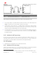

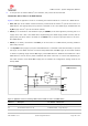


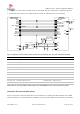
Table Of Contents
- Contents
- 1 System description
- 1.1 Overview
- 1.2 Architecture
- 1.3 Pin-out
- 1.4 Operating modes
- 1.5 Supply interfaces
- 1.5.1 Module supply input (VCC)
- 1.5.1.1 VCC supply requirements
- 1.5.1.2 VCC current consumption in 2G connected mode
- 1.5.1.3 VCC current consumption in 3G connected mode
- 1.5.1.4 VCC current consumption in LTE connected mode
- 1.5.1.5 VCC current consumption in cyclic low power idle mode / active mode
- 1.5.1.6 VCC current consumption in fixed active mode
- 1.5.2 Generic digital interfaces supply output (V_INT)
- 1.5.1 Module supply input (VCC)
- 1.6 System function interfaces
- 1.7 Antenna interfaces
- 1.8 SIM interfaces
- 1.9 Data communication interfaces
- 1.10 eMMC interface
- 1.11 Digital Audio interfaces
- 1.12 ADC interfaces
- 1.13 General Purpose Input/Output
- 1.14 Reserved pins (RSVD)
- 1.15 System features
- 1.15.1 Network indication
- 1.15.2 Jamming detection
- 1.15.3 IP modes of operation
- 1.15.4 Dual stack IPv4 and IPv6
- 1.15.5 Embedded TCP/IP and UDP/IP
- 1.15.6 Embedded FTP and FTPS
- 1.15.7 Embedded HTTP and HTTPS
- 1.15.8 SSL and TLS
- 1.15.9 Firmware update Over AT (FOAT)
- 1.15.10 Firmware update Over The Air (FOTA)
- 1.15.11 Power Saving
- 2 Design-in
- 2.1 Overview
- 2.2 Supply interfaces
- 2.2.1 Module supply (VCC)
- 2.2.1.1 General guidelines for VCC supply circuit selection and design
- 2.2.1.2 Guidelines for VCC supply circuit design using a switching regulator
- 2.2.1.3 Guidelines for VCC supply circuit design using a LDO linear regulator
- 2.2.1.4 Guidelines for VCC supply circuit design using a rechargeable battery
- 2.2.1.5 Guidelines for VCC supply circuit design using a primary battery
- 2.2.1.6 Additional guidelines for VCC supply circuit design
- 2.2.1.7 Guidelines for the external battery charging circuit
- 2.2.1.8 Guidelines for external charging and power path management circuit
- 2.2.1.9 Guidelines for removing VCC supply
- 2.2.1.10 Guidelines for VCC supply layout design
- 2.2.1.11 Guidelines for grounding layout design
- 2.2.2 Generic digital interfaces supply output (V_INT)
- 2.2.1 Module supply (VCC)
- 2.3 System functions interfaces
- 2.4 Antenna interface
- 2.5 SIM interfaces
- 2.6 Data communication interfaces
- 2.7 eMMC interface
- 2.8 Digital Audio interface
- 2.9 ADC interfaces
- 2.10 General Purpose Input/Output
- 2.11 Reserved pins (RSVD)
- 2.12 Module placement
- 2.13 Module footprint and paste mask
- 2.14 Thermal guidelines
- 2.15 Design-in checklist
- 3 Handling and soldering
- 4 Approvals
- 5 Product testing
- 6 FCC Notes
- Appendix
- Glossary
- Related documents
- Revision history
- Contact

TOBY-L3 series - System Integration Manual
TSD-19090601 - R13 System Integration Manual Page 103 of 143
☞ Connect the DDC (I
2
C) pull-ups to the V_INT 1.8 V supply source, or another 1.8 V supply source enabled
after V_INT (e.g., as the GNSS 1.8 V supply present in Figure 51 application circuit), as any external
signal connected to the DDC (I
2
C) interface must not be set high before the switch-on of the V_INT
supply of DDC (I
2
C) pins, to avoid latch-up of circuits and allow a clean boot of the module.
The signal shape is defined by the values of the pull-up resistors and the bus capacitance. Long wires on
the bus will increase the capacitance. If the bus capacitance is increased, use pull-up resistors with a nominal
resistance value lower than 4.7 k, to match the I
2
C bus specifications [7] regarding the rise and fall times
of the signals.
Figure 50 and Table 38 describe typical application circuits for connecting TOBY-L3 series modules to 1.8
V I2C devices (see Figure 50 top side) or 3 V I2C devices (see Figure 50 bottom side).
1.8V I2C Device
SDA
SCL
1V8
5
V_INT
R1 R2
1V8 1V8
SDAx
SCLx
TOBY-L3 series
R1 R2
3V0
SDAx
SCLx
R3 R4
1V8
SDA_A SDA_B
GND
U1
SCL_A
SCL_B
VCCA
VCCB
I2C-bus Bidirectional
Voltage Translator
5
V_INT
C1
C2
SDA
SCL
OE
GND GND
3V I2C Device
TOBY-L3 series
GND GND
Figure 50: Application circuit for connecting TOBY-L3 series modules to 1.8 V or 3 V I2C devices
Reference
Description
Part Number - Manufacturer
R1, R2, R3, R4
4.7 k Resistor 0402 5% 0.1 W
RC0402JR-074K7L - Yageo Phycomp
C1, C2
100 nF Capacitor Ceramic X7R 0402 10% 16 V
GRM155R71C104KA01 - Murata
U1
I2C-bus Bidirectional Voltage Translator
TCA9406DCUR
10
- Texas Instruments
Table 38: Components for connecting TOBY-L3 series modules to 1.8 V or 3 V I2C devices
☞ The ESD sensitivity rating of the DDC (I
2
C) pins is 1 kV (HBM according to JESD22-A114). A higher
protection level could be required if the lines are externally accessible and it can be achieved by
mounting an ESD protection (e.g. EPCOS CA05P4S14THSG) close to the accessible points.
10
Voltage translator providing partial power down feature: the external 3 V supply can be ramped up before V_INT 1.8 V supply