
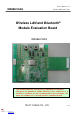
User Manual


22-Jun.2020 Ver.1.5
TAIYO YUDEN CO., LTD.
TAIYO YUDEN CO., LTD. 5 / 10
WBSBHVGXG
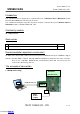
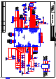
Evaluation board layout
Pin description of evaluation board
WBSBHVGXG (TE8561-1)
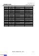
CN1: DC Power Supply
No.
Pin name
Direction
Description
1
5V
Input
5.0V input.
2
GND
GND
Ground
CN2: VIO Voltage Select (Default Setting: 1-2 short.)
No.
Pin name
Direction
Description
1
3.3V
Output
3.3V output.
2
VIO
Input
Input for VIO.
3
1.8V
Output
1.8V output.
CN3: VIO_SD Voltage Select (Default Setting: 2-3 short.)
No.
Pin name
Direction
Description
1
3.3V
Output
3.3V output.
2
VIO
Input
Input for VIO_SD.
3
1.8V
Output
1.8V output.
CN3: VIO_SD voltage select
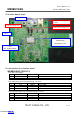
WLAN and Bluetooth Module
(WYSBHVGXG)
NXP 88W8887 module
CN1: DC power supply (5V)
(Default)
CN2: VIO voltage select
CN9:
ANT_CN(WLAN/BTRF)
ANT 1
SW1: Reset SW
Downloaded from Arrow.com.Downloaded from Arrow.com.Downloaded from Arrow.com.Downloaded from Arrow.com.Downloaded from Arrow.com.