
Datasheet


TS78M00 Series
Taiwan Semiconductor
2 Version: F1512
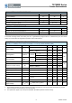
ABSOLUTE MAXIMUM RATINGS
PARAMETER SYMBOL LIMIT UNIT
DC Input Voltage V
IN
35
V
Power Dissipation
P
D
Internally Limited W
Operating Junction Temperature Range T
J
0 ~ +150
o
C
Storage Temperature Range
T
STG
-65~+150
o
C
THERMAL PERFORMANCE
PARAMETER SYMBOL LIMIT UNIT
Junction to Case Thermal Resistance
R
ӨJC
10
°C/W
Junction to Ambient Thermal Resistance
R
ӨJA
100 °C/W
Notes: R
ӨJA
is the sum of the junction-to-case and case-to-ambient thermal resistances. The case thermal reference is defined
at the solder mounting surface of the drain pins. R
ӨJA
is guaranteed by design while R
ӨCA
is determined by the user’s board
design. R
ӨJA
shown below for single device operation on FR-4 PCB in still air.
ELECTRICAL SPECIFICATIONS
TS7
8M05
(V
IN
=10V, I
OUT
=350mA, 0
o
C≤T
J
≤125
o
C, C
IN
=0.33µF, C
OUT
=0.1µF, unless otherwise noted)
PARAMETER SYMBOL
CONDITION MIN TYP MAX
UNIT
Output voltage V
OUT
T
J
=25°C
4.80 5 5.20
V
7.5V≤V
IN
≤20V
5mA≤I
OUT
≤350mA
4.75 5 5.25
Line Regulation REG
LINE
T
J
=25°C
7.5V≤V
IN
≤25V
-- 3 100
mV
8V≤V
IN
≤12V
-- 1 50
Load Regulation REG
LOAD
T
J
=25°C
5mA≤I
OUT
≤500mA
-- 15 100
5mA≤I
OUT
≤200mA
-- 5 50
Quiescent Current I
Q
I
OUT
=0, T
J
=25°C
-- 3 6
mA
Quiescent Current Change ΔI
Q
7.5V≤V
IN
≤25V
-- -- 0.8
5mA≤I
OUT
≤350mA
-- -- 0.5
Output Noise Voltage V
N
10Hz≤f≤100KHz, T
J
=25°C
-- 40 -- µV
Ripple Rejection Ratio RR f=120Hz, 8V≤V
IN
≤18V
62 78 -- dB
Voltage Drop V
DROP
I
OUT
=500mA, T
J
=25°C
-- 2 -- V
Output Resistance R
OUT
f=1kHz
-- 17 -- mΩ
Output Short Circuit
Current
I
OS
T
J
=25°C -- 50 -- mA
Peak Output Current I
O
peak T
J
=25°C
-- 0.7 -- A
Temperature Coefficient of
Output Voltage
ΔV
OUT
/ΔT
J
I
OUT
= 5mA, 0°C≤T
J
≤125°C -- -0.2 -- mV/°C
Note:
1. Pulse testing techniques are used to maintain the junction temperature as close to the ambient temperature as possible,
and thermal effects must be taken into account separately
2. This specification applies only for DC power dissipation permitted by absolute maximum ratings.