
Datasheet

TS317
3-Terminal Adjustable Positive Voltage Regulator
Document Number:
DS_P0000263
2
Version: E15
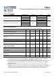
Thermal Performance
Condition Package type
Symbol
Typ Unit
Thermal Resistance Junction to Air
TO-220
RΘ
JA
50
°C/W
TO-263 55
TO-252 100
SOT-223 130
Thermal Resistance Junction to Case
TO-220
RΘ
JC
5
°C/W
TO-263 5
TO-252 10
SOT-223 15
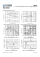
Electrical Characteristics
(V
I
-V
O
= 5.0 V, Io=500mA for TO-220/TO-263 packages, Io=200mA for TO-252/SOT-223 package)
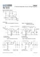
Parameter Figure
Symbol Min. Typ. Max. Unit
Reference voltage, 3V ≤ Vi-Vo ≤ 40V
10mA ≤ Io ≤ Imax, Pd ≤ Pmax,
3 Vref 1.20 1.25 1.30 V
Line regulation (Note 3)
Ta = 25
°C, 3V≤Vi-Vo≤40V
1 REGline -- 0.01 0.07 %/V
Load regulation Ta = 25
°C, 10mA ≤ I
O
≤ Imax (Note 2)
V
O
≤ 5.0
V
O
≥ 5.0
2 REGload
--
--
5.0
0.1
25
0.5
mV
%V
Thermal regulation, Ta = 25°C (Note 5), 20mS Pulse REGtherm
-- 0.03 0.07 %Vo/W
Adjustment pin current 3 Iadj -- 50 100 uA
Adjustment pin current change, 3V ≤ V
I
- V
O
≤ 40V
10mA ≤ Io ≤ Imax, Pd ≤ Pmax,
1.2
∆Iadj
-- 0.2 5.0 uA
Maximum output current, V
I
- V
O
≤ 15V, Pd ≤ Pmax
TO-220 / TO-263 Package
TO-252 / SOT-223 Package
3 Imax
1.5
0.5
--
--
--
--
A
Temperature stability (T
LOW
≤ Tj ≤ T
HIGH
) 3 T
S
-- 1 -- % Vo
Minimum load current to maintain regulation
(V
I
- V
O
= 40 V)
3 ILmin -- 3.5 10 mA
RMS Noise, % of V
O
,
Ta =25
°C, 10Hz
≤ f ≤ 10KHz N -- 0.003
-- % Vo
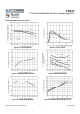
Ripple Rejection, Vo =10V, f =120Hz (Note 3)
Without Cadj
Cadj = 10uF
4 PSRR
--
66
65
80
--
--
dB
Long-term stability (Note 4), Tj
= 125°C, 1000hrs 3 S -- 0.3 1.0 %
Notes: 1. T
LOW
to T
HIGH
= 0°C to +125°C, Pmax is internally limited
2. Load and line regulation are specified at constant junction temperature. Changes in V
O
due to heating
effects must be taken into account separately. Pulse testing with low duty cycle is used.
3. Cadj, when used, is connected between the adjustment pin and ground. Since Long-Term Stability cannot
be measured on each device before shipment, this specification is an engineering estimate of average
stability from lot to lot.
4. Power dissipation within an IC voltage regulator produces a temperature gradient on the die, affecting
individual IC components on the die. These effects can be minimized by proper integrated circuit design and
layout techniques. Thermal Regulation in the effect of these temperature gradients on the output voltage
and is expressed in the percentage of output change per watt of power change in a specified time.