
User Manual
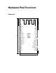
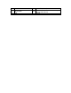
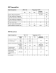

PCB Footprint
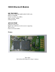
1.0
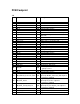
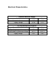
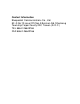
No.
Symbol
I/O
Description
1 GND - Ground
2 VDD_PA I No connection
3 GND - Ground
4 AIO(0) I/O
Programmable I/O line
5 AIO(1) I/O
Programmable I/O line
6 RESET I Reset if low
7 SPI_MISO O Synchronous serial interface data output
8 SPI_CSB I
Chip select for Synchronous Serial Interface
active low
9 SPI_CLK I Synchronous serial interface clock
10 SPI_MOSI I Synchronous serial interface data input
11 UART_CTS I UART clear to send active low
12 UART_TX O UART data output
13 UART_RTS O UART request to send active low
14 UART_RX I UART data input
15 1V8OUT O 1.8V output voltage
16 VDD I 3.3V input voltage
17 GND - Ground
18 PIO(11) I/O
Programmable I/O line
19 PIO(10) I/O
Programmable I/O line
20 PIO(9) I/O
Programmable I/O line
21 PIO(8) I/O
Programmable I/O line
22 PCM_OUT O Synchronous data out
23 PCM_SYNC I/O
Synchronous data sync
24 PCM_IN I Synchronous data input
25 PCM_CLK I/O
Synchronous data clock
26 USB_DP I/O
USB data plus with selectable internal 1.5k
Ω
pull-up resistor
27 USB_DN I/O
USB data minus
28 PIO(7) I/O
Programmable I/O line
29 PIO(6)/WLAN_Active/Ch_Data
I/O
Programmable I/O line or
Optionally WLAN_Acitve/Ch_Data input for
co-existence signaling
30 PIO(5)/BT_Active I/O
Programmable I/O line or
Optionally BT_Acitve output for
co-existence signaling
31 PIO(4)/BT_Priority/Ch_Clk I/O
Programmable I/O line or
Optionally BT_Priority/Ch_Clk output for
co-existence signaling
32 PIO(3) I/O
Programmable I/O line
33 PIO(2) I/O
Programmable I/O line
34 PIO(1)/TXEN I/O
Programmable I/O line or Control output for