
SB4002A_Data Sheet_EN


SB4002A
81
8.2 Legacy Bus Timing Specifications
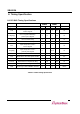
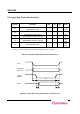
Table 8-2. Legacy Bus Timing Specifications for Write Access
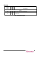
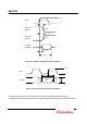
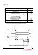
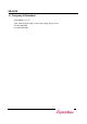
CS#
Td4
MEMW#
Td2
Td3
Tw1Td1
DATA
IOW#
BYTE_EN
ADDRESS
Figure 8-3. Legacy Bus Timing Specifications for Write Access
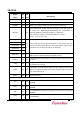
Symbol
Parameter
Min
Typ
Max
Units
Td1
CS#/EA/BYTE_EN# assert to
IOW#/MEMW# assert
-
1
-
PCI
CLK
Td2
IOW#/MEMW# deassrt to
CS#/EA/BYTE_EN# deassert
-
1
-
PCI
CLK
Td3
IOW#/MEMW# enable to ED valid
-
-
3
ns
Td4
IOW#/MEMW# disable to ED valid
-
1
-
PCI
CLK
Tw1
IOW#/MEMW# width
-
n
-
PCI
CLK
* ‘n’ meams IOW#/MEMW# signal width is ‘n’ times PCI CLK.
‘n’ would be determined by Base Address Space Setting Register[10:8], Refer to Chapter 6