
SB4002A_Data Sheet_EN


SB4002A
8
2. PCI BUS
2.1 PCI Bus Protocol
2.1.1 PCI Feature
- PCI is a synchronous bus which supports 33MHz/66MHz clock and 32-bit/64-bit data path.
(SB4002A supports 33MHz/66MHz clock and 32-bit data path.)
- PCI increases transmission efficiency via Linear/Cacheline wrap burst access. (SB4002A
supports linear burst access.)
- PCI supports plug & play, and automatically reads the required resources from BIOS/OS and
allocates them to the device.
- PCI provides high reliability of bus by supporting parity checking and target termination.
- PCI multiplexes the address/data pins to increase efficiency of chip package.
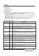
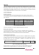
2.1.2 PCI Signal Description
Signal name
Type
Description
CLK
in
Provides timing for all actions of PCI bus. The signal gives input for all the PCI
devices, and its rising edge becomes the reference for input/output and timing
constant of all signals. (exception: RST#, INTx#, PME#, CLKRUN#)
RST#
in
The reset signal of the PCI system.
AD[31:0]
t/s
Address/Data multiplexed signal. This signal is used during the PCI
transmission as the address signal in the address phase or as the data signal
in the data phrase.
C/BE[3:0]#
t/s
Bus Command/Byte Enable multiplexed signal. It is used during the PCI
transmission as BUS Command in the address phase or as Byte Enable in the
data phrase.
PAR
t/s
Provides the even parity for AD[31:0] and C/BE[3:0].
FRAME#
s/t/s
Indicates beginning and duration of PCI access.
IRDY#
s/t/s
Initiator Ready. The signal indicates the bus master’s ability to complete the
current data phase of the transaction.
TRDY#
s/t/s
Target Ready. The signal indicates the target device’s ability to complete the
current data phase of the transaction.
STOP#
s/t/s
Indicates the current target is requesting the master to stop the current
transaction.
LOCK#
s/t/s
Provides for the exclusive use of a resource.
IDSEL
in
Indicates that a device is selected during configuration read and write
transactions.