
SB4002A_Data Sheet_EN

SB4002A
74
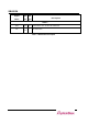
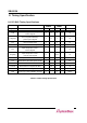
Signal
Name
Pin
No.
Pin
Type
Description
IOW#
148
out
I/O Write Signal. Asserted at write access in the I/O port.
MEMR#
153
out
Memory Read Signal. Asserted at read access in the memory.
MEMW#
152
out
Memory Write Signal. Asserted at write access in the memory.
BE[3:0]#
-
out
Byte Enable Signal. Enable signal for each byte of the data signal on
the Legacy bus. BE[3]#,BE[2]#,BE[1]#,BE[0]# are corresponding to
ED[31:24], ED[23:16], ED[15:8] and ED[7:0], respectively.
If the data path is in bytes, no substantial influence is made.
(Pin No. : 101, 112, 126, 135)
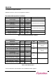
INT1GPIO0
24
in
/
bi
The interrupt request and general purpose I/O port muxed pin. The
Muxed Pin Select Register [15:11] in the control register space is used
to determine the use of the pin (INT pin or GPIO pin)
INT2GPIO1
25
INT3GPIO2
26
INT4GPIO3
27
INT5GPIO4
28
PME_REQ
100
in
Power Management Event Request Signal. The signal asserts the
PME# signal to request the power management event.
PME_S
99
out
Power Management Status Signal. The signal reports the power state of
the device.
HSW
98
in
CompactPCI Hot Swap Switch Signal. The pin receives the switch input
for insert/eject at hot swap.
HLED
95
out
CompactPCI Hot Swap Switch Signal. The pin outputs the LED on/off
signal for insert/eject complete at hot swap. The LOO value of HS_CSR
in the configuration is out.
OPCLK
113
out
Output of PCI clock.
Serial EEPROM Interface Signal
RCS
94
out
Serial EEPROM Chip Select Signal. Connected to CS of the Serial
EEPROM.
RSK
93
out
Serial EEPROM Serial Data Clock Signal. Connected to SK of the Serial
EEPROM.
RDI
90
in
Serial EEPROM Serial Data Input Signal. Connected to DO of the Serial
EEPROM.
RDO
89
out
Serial EEPROM Serial Data Output Signal. Connected to DI of the
Serial EEPROM.