
SB4002A_Data Sheet_EN


SB4002A
73
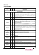
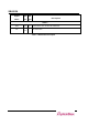
Signal
Name
Pin
No.
Pin
Type
Description
INTA#
31
o/d
PCI interrupt signal.
PME#
34
o/d
Power Management Event. Requests change of power state of a device
or a system. Enabled when the power management interface capability
is supported.
ENUM#
88
o/d
Enumeration. Shows that the board has been inserted to the system, or
is about to be removed. This is enabled when the CompactPCI Hot
Swap is supported.
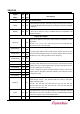
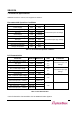
Legacy Bus Signal
EA[22:0]
-
out
Legacy Bus Address. The lower 26-bit output at transaction on the
Legacy bus.
(Pin No. : 8, 7, 6, 5, 4, 3, 2, 1, 176, 175, 174, 173, 172, 169, 168, 167,
165, 164, 161, 160, 159, 158, 155)
GPIO7/EA[23]
9
bi
/out
The Legacy Bus Address and General Purpose I/O Port muxed pin. The
Muxed Pin Select Register [10:8] in the control register space is used to
determine the use of the pin (address pin or GPIO pin).
GPIO6/EA[24]
10
bi
/out
GPIO5/EA[25]
13
bi
/out
CSX#/EA[26]
14
out
The Legacy Bus Address and CSn# muxed pin. The Muxed Pin Select
Register [5:0] in the control register space is used to determine the use
of the pin (address pin or CSn# pin)
In CSn#, n indicates the order of the base address spaces. If the control
register space is allocated to the base address5, the CS5# pin function
is changed to CS0#.
CS5#/CS0#/EA[27]
15
out
CS4#/EA[28]
16
out
CS3#/EA[29]
17
out
CS2#/EA[30]
18
out
CS1#/EA[31]
166
out
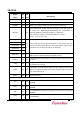
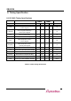
ED[31:0]
-
bi
Legacy Bus Data. Data for the Legacy bus transaction is input and
output through this pin. The effective data line varies by data path,
endian and byte enable.
(Pin No. : 102, 103, 104, 105, 108, 109, 110, 111, 114, 115, 116, 119,
120, 121, 122, 123, 127, 128, 129, 130, 131, 132, 133, 134, 138, 139,
140, 141, 142, 145, 146, 147)
RST#
154
out
Legacy Bus Reset. The reset signal output to the Legacy bus. Asserted
when PRST# of PCI bus is asserted. It is also asserted if 52h is written
on the reset register of the control register space.
IOR#
151
out
I/O Read Signal. Asserted at read access in the I/O port.