
SB4002A_Data Sheet_EN


SB4002A
66
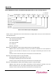
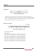
GPIO Output Register
47
GO6 GO0
2
GO4
3
GO1GO2
1
GO5 GO3
R = Reserved
6
R
05
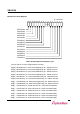
Table 6-5. GPIO Output Register Layout
Sets output of each GPIO.
Bit[7] : Reserved
Bit[6] : GO6, Sets the output of GPIO6.
Bit[5] : GO5, Sets the output of GPIO5.
Bit[4] : GO4, Sets the output of GPIO4.
Bit[3] : GO3, Sets the output of GPIO3.
Bit[2] : GO2, Sets the output of GPIO2.
Bit[1] : GO1, Sets the output of GPIO1.
Bit[0] : GO0, Sets the output of GPIO0.
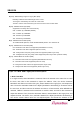
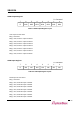
GPIO Input Register
6
GI3
2
R = Reserved
357 0
GI5 GI4GI6R
14
GI0GI2 GI1
Table 6-6. GPIO Input Register Layout
Reads input of each GPIO.
Bit[7] : Reserved
Bit[6] : GI6, Reads the input of GPIO6.
Bit[5] : GI5, Reads the input of GPIO5.
Bit[4] : GI4, Reads the input of GPIO4.
Bit[3] : GI3, Reads the input of GPIO3.
Bit[2] : GI2, Reads the input of GPIO2.
Bit[1] : GI1, Reads the input of GPIO1.
Bit[0] : GI0, Reads the input of GPIO0.