
SB4002A_Data Sheet_EN


SB4002A
65
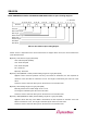
Reset Register
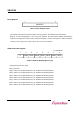
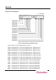
SW RESET
07
Table 6-3. Reset Register Layout
This register resets the chip internal register and Legacy bus in the software level. (Write Only)
Bit[7:0] : If 52h corresponding to “R" is used, the default is the chip internal register (excluding the
register on Configuration Space Header and Reset Register), and the reset signal is output through the
reset pin on the Legacy bus. If other values are used, reset is released.
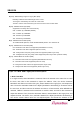
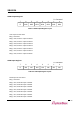
GPIO Out Enable Register
3
GEN4 GEN2GEN3
5
R
6
GEN0GEN1
R = Reserved
2
GEN6
4 01
GEN5
7
Table 6-4. GPIO Out Enable Register Layout
Sets input/output of each GPIO.
Bit[7] : Reserved
Bit[6] : GEN6, 1b : Enables GPIO6 Out, 0b : Disables GPIO6 Out(Default)
Bit[5] : GEN5, 1b : Enables GPIO5 Out, 0b : Disables GPIO5 Out(Default)
Bit[4] : GEN4, 1b : Enables GPIO4 Out, 0b : Disables GPIO4 Out(Default)
Bit[3] : GEN3, 1b : Enables GPIO3 Out, 0b : Disables GPIO3 Out(Default)
Bit[2] : GEN2, 1b : Enables GPIO2 Out, 0b : Disables GPIO2 Out(Default)
Bit[1] : GEN1, 1b : Enables GPIO1 Out, 0b : Disables GPIO1 Out(Default)
Bit[0] : GEN0, 1b : Enables GPIO0 Out, 0b : Disables GPIO0 Out(Default)