
SB4002A_Data Sheet_EN


SB4002A
63
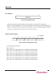
Legacy bus. The device deasserts TRDY# at the next CLK, asserts IOW# on the Legacy bus,
and outputs the data. Then, the above procedure is repeated. Therefore, the TRDY# to
TRDY# wait cycle on the PCI bus is bit[9:7]+bit[15:13]+10b.
2. Delayed Time Write
In a single transfer, when DEVSEL# is asserted, TRDY# is asserted at the same time to catch
the data, and the device ends the PCI cycle. After an appropriate time period, the device
asserts CS# and approves the address and data. The device asserts IOW# at the next CLK,
and maintains IOW# for the bit[9:7]+001b before deasserting it. The device deasserts CS# and
removes the address and data at the next CLK.
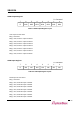
In a burst transfer, when DEVSEL# is asserted, the device asserts TRDY#, and executes the
burst cycle in no wait (but within the size of FIFO). After an appropriate time period, the
device asserts CS# and approves the address and data. The device asserts IOW# at the next
CLK, maintains IOW# for the bit[9:7]+001b before deasserting it, and outputs the data. Then
the above procedure is repeated. Therefore the wait cycle on the PCI bus is 0.
If a cycle is executed on the PCI bus before a cycle is finished on a Legacy bus, the device
terminates the transaction with retry.
3. Real Time Read
In a single transfer, the device asserts DEVSEL#, outputs the address, and asserts CS#. The
device asserts IOR# at the next CLK, maintains IOR# for the bit[12:10], and asserts TRDY#.
The device deasserts IOR#, TRDY# and DEVSEL# at the next CLK, and then, at the next
CLK, deasserts CS# and removes the address.
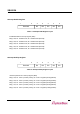
In a burst transfer, the device asserts DEVSEL#, outputs the address, and asserts CS#. The
device asserts IOR# at the next CLK, maintains IOR# for the bit[12:10], and asserts TRDY# at
the next CLK. At the following CLK, the device deasserts IOR#, and after bit[18:16]+2, asserts
IOR#. After the time for the bit[12:10], the device asserts TRDY#. At the next CLK, the device
deasserts IOR# and TRDY#. Then, the above procedure is repeated. Therefore the TRDY# to
TRDY# wait cycle on the PCI bus is bit[12:10]+bit[18:16]+2.
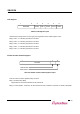
4. Delayed Time Read without Prefetch
It is applied to a single transfer only. On receiving the initial access, the device stores the
address and command, finishes the PCI bus cycle with retry, and after an appropriate time
period, executes a read transaction on the Legacy bus. Where, the length of IOR# is bit[12:10]
+1. Then, if the same cycle is started on the PCI bus, the device responds to the cycle in no
wait.