
SB4002A_Data Sheet_EN


SB4002A
61
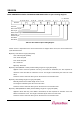
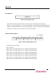
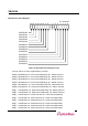
BASE ADDRESS1/2/3/4/5 & EXPANSION ROM BASE Address Space Setting Register
R
WR# Length
1
WR# to WR# Length
1124 21023 315
Write Mode
RD# Length
814
Read Mode
R
22 12
Prefetch Length
31 20 719 4
R
R = Reserved
6 0
Reserved
Data Path
1826 1625
RD# to RD# Langth
RR
Table 6-2. Base Address Space Setting Register
If burst access is requested for the device which does not support burst access, the device finishes the
cycle with Disconnect.
Bit[25:24] : Data Path for Legacy Bus (R/W)
00b : 8-bit data path (Default)
01b : 16-bit data path
10b : 32-bit data path
11b : Reserved
bit[31:22] : Reserved
Bit[22:20] : RD# (MEMR# or IOR#) to RD# Adding Length for Legacy Bus (R/W)
Applied to burst read and prefetch read only. Once WR# is deasserted, the time required for
assertion of the next WR# is at least PCI 2 CLK. The length is extended by the value set in this
value.
This bit is used to control the wait cycle on the PCI bus in the real time write.
Bit[18:16] : RD# Adding Length for Legacy Bus (R/W)
Basically, WR# has the enable length of PCI 1 CLK.
The length is extended by the value set in this value.
This bit is used to control the wait cycle on the PCI bus in the real time write.
Bit[14:12] : WR# (MEMW# or IOW#) to WR# Adding Length for Legacy Bus (R/W)
Applied to burst write only. Once WR# is deasserted, the time required for assertion of the next
WR# is at least PCI 2 CLK. The length is extended by the value set in this value.
This bit is used to control the wait cycle on the PCI bus in the real time write.