
SB4002A_Data Sheet_EN

SB4002A
60
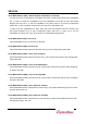
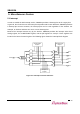
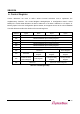
6. Control Register
Theses addresses are used to define various internal selections and to implement the
supplementary functions. The Control Register Setting0/1(See 4. Configuration Data in Serial
ROM)of the Serial ROM allocates the Base Address0 or the Base Address5 to I/O Space or
Memory Space in the PCI Configuration Space Header, and supports access to the unit of DWORD.
The table below describes the details of the Control Registers.
Address
Byte3
Byte2
Byte1
Byte0
00h
BASE ADDRESS1 Space Setting Register
04h
BASE ADDRESS2 Space Setting Register
08h
BASE ADDRESS3 Space Setting Register
0Ch
BASE ADDRESS4 Space Setting Register
10h
BASE ADDRESS5 Space Setting Register
14h
EXPANSION ROM BASE Address space Setting Register
18h
Reserved
Reset Register
1Ch
Reserved
GPIO Input
Register
GPIO Output
Register
GPIO Out Enable
Register
20h
Endian & LOCK
Control Register
Poll Register
Interrupt Polarity
Register
Interrupt Enable
Register
24h
Reserved
Muxed Pin Control Register
Table 6-1. Control Register Map