
SB4002A_Data Sheet_EN

SB4002A
46
3.4 Endian Conversion
The data are divided into Little Endian and Big Endian depending on the order or BYTE lanes in
the system structure.
In case of a DWORD system with the [31:0] data path, in Little Endian, [31:24], [23:16], [15:8] and
[7:0] are the fourth, third, second and first byte, respectively. In Big Endian, [7:0], [15:8] and [23:16]
are the fourth, third and fourth byte, respectively.
Basically, PCI bus is based on Little Endian. However, because the device connected to the
Legacy bus can be the device that supports Little Endian, SB4002A supports conversion of the
Little Endian data into the Big Endian data. The following tables show the conversion methods.
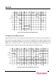
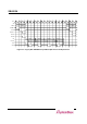
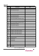
- DWORD Data path
Byte Lane
BYTE3
BYTE2
BYTE2
BYTE0
Little Endian
PCI bus
AD[31:24]
AD[23:16]
AD[15:8]
AD[7:0]
Little Endian
Lagacy bus
ED[31:24]
ED[23:16]
ED[15:8]
ED[7:0]
Big Endian
Lagacy bus
ED[7:0]
ED[15:8]
ED[23:16]
ED[31:24]
Table 3-1. DWORD Data path Endian Conversion
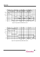
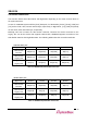
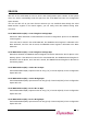
- WORD Data path
Byte Lane
BYTE3
BYTE2
BYTE2
BYTE0
Little Endian
PCI bus
AD[31:24]
AD[23:16]
AD[15:8]
AD[7:0]
Little Endian
Lagacy bus
ED[15:8]
ED[7:0]
ED[15:8]
ED[7:0]
Big Endian
Lagacy bus
ED[7:0]
ED[15:8]
ED[7:0]
ED[15:8]
Table 3-2. WORD Data path Endian Conversion