
SB4002A_Data Sheet_EN


SB4002A
39
3. Legacy Bus
SB4002A provides the ISA like Legacy bus at the back end, in order that it can interface with
general devices via interworking with PCI bus. SB4002A provides the chip select signal (CSx#), I/O
read/write(IOR#, IOW#) and memory read/write#(MEMR#, MEMW#) signal to support the general
devices.
SB4002A also supports a variety of flexible accessing methods.
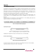
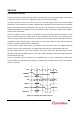
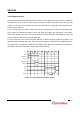
3.1 Real Access/Delayed Access
3.1.1 Real Access
This method provides the real time data transfer by executing the PCI transaction and the Legacy
bus transaction at the same time.
At the same time it is hit, the device sends the address signal, the chip select signal and the R/W
signal, and then, depending on R/W, outputs the data on the PCI bus to the Legacy bus, or vice
versa.
For the write process, because it is not necessary that the transaction on the PCI bus is extended
until the transaction on the Legacy bus is completed, the device completes the transaction on the
PCI bus as soon as possible, stores the write data on the buffer, and starts the transaction on the
Legacy bus.
For the read process, because the device can send the valid data to the PCI bus at the time the
transaction on the Legacy bus is completed, a wait cycle must be inserted to the PCI bus.
AD
IRDY#
EA
TRDY#
IOW#
CLK
IOR#
CS#
ED
DEVSEL#
FRAME#
Figure 3-1. Legacy Bus Real Access