
SB4002A_Data Sheet_EN

SB4002A
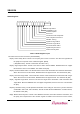
30
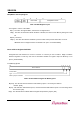
PMC(Power Management Capabilities) Register
Aux_Current
D1_Support
011
VersionPME_Support
10
PME Clock
8 5
DSI
23
Reserved
6 49
D2_Support
15
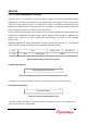
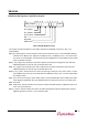
Table 2-28. PMC Register Layout
This register contains information on the power management capability of the device. [RO : non-
downloadable]
Bit[15:11] : PME Support. This bit shows the power state in which the device can assert PME#. Bit[11] is
allocated to D0, Bit[12] to D1, Bit[13] to D2, Bit[14] to D3
hot
, and Bit[15] to D3
cold
, The value is 1b if
the device can assert PME#, or 0b otherwise. Because SB4002A can assert PME# in D0 and D3
hot
state, the default is 01001b.
Bit[10] : D2_Support. This bit shows if the device supports the D2 power management state. Because
SB4002A supports D0 and D3 only, the default value is 0b.
Bit[9] : D1_Support. This bit shows if the device supports the D1 power management state. Because
SB4002A supports D0 and D3 only, the default value is 0b.
Bit[8:6] : Aux_Current. This bit shows the current used through 3.3Vaux pin. If the device in D3
cold
cannot
assert PME#, the bit must be set to 000b. Because SB4002A, when in D3
cold,
cannot assert PME#,
the default is 000b.
Bit[5] : DSI. This bit is used by the device which requires a special initialization process before the device
driver-triggered initialization. Because SB4002A does not support this process, the default is 0b.
Bit[4] : Reserved.
Bit[3] : PME Clock. This bit indicates if a PCI clock is required for PME# assertion. SB4002 uses the PCI
clock, and the default is 1b.
Bit[2:0] : Version. This bit indicates the version of Power Management Interface Specification. Because
SB4002 supports the version 1.1, the default is 010b.