
SB4002A_Data Sheet_EN

SB4002A
28
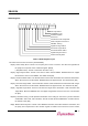
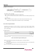
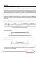
Interrupt Pin Register
7
Interrupt Pin
0
Table 2-22. Interrupt Pin Register Layout
This register indicates the PCI interrupt pin used by the device. Because SB4002A is a single function, the
default value is set to 1h via INTA#. [RO : non-downloadable]
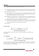
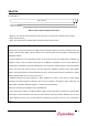
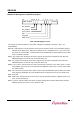
MIN_GNT Register
MIN_GNT
7 0
Table 2-23. MIN_GNT Register Layout
This register indicates the time required for burst access. Because SB4002A does not support this register,
the default is 00h. [RO : non-downloadable]
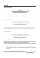
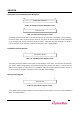
MAX_LAT Register
7 0
MAX_LAT
Table 2-24. MAX_LAT Register Layout
This register indicates the frequency of access to the PCI bus. Because SB4002A does not support this
register, the default is 00h. [RO : non-downloadable]