
SB4002A_Data Sheet_EN

SB4002A
24
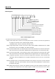
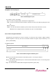
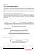
Cache Line Size Register
0
Cache Line Size
7
Table 2-12. Cache Line Size Register Layout
The register designates the size of the cache line of the system. Since this register is for the
master, SB4002A does not support this register. The default is 0b. [RO : non-downloadable]
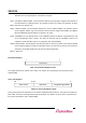
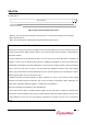
Latency Timer Register
Latency Timer
07
Table 2-13. Latency Timer Register Layout
The register designates the latency clock for the bus master that executes a burst access. Since this register
is for the master, SB4002A does not support this register. The default is 0b. [RO : non-downloadable]
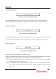
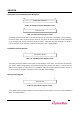
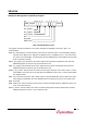
Header Type Register
7
Header Type
0
Table 2-14. Header Type Register Layout
Configuration Space Header Type [RO : non-downloadable]
Header Type register identifies the layout of second part of the predefined header(beginning at byte 10h in
Configuration Space) and also whether or not the device contains multiple functions.
Bit[7] : This bit indicates whether the device supports multi-function or single function. Because SB4002A
supports single function, the default is 0b.
Bit[6:0] : This bit identify the layout of second part of the predefined header. 00h is the target device, 01h is
the PCI-to-PCI bridge, and 02h is the Cardbus bridge. Because SB4002A is a target device, the
default is 00.