
SB4002A_Data Sheet_EN

SB4002A
21
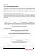
Bit[9] : Fast Back-to-Back Enable. The bit indicates capability of fast back-to-back transaction between
the master and other devices. This is activated when all the targets on the bus support fast back-
to-back transaction. The value 1b indicates that the master supports fast back-to-back
transaction with other device, while 0b indicates that the master does not support fast back-to-
back transaction. Since this bit is for the master, SB4002A does not support this bit. The default
is 0b. [RO]
Bit[8] : SERR# Enable. The enable bit for SERR# driver. The value 1b enables the target to assert
SERR#, and 0b disables assertion of SERR#. The default is 0b. [RO]
Bit[7] : Stepping Control. The bit indicates whether or not the device supports address/data stepping.
The default is 0b. [R] (* Not supported in PCI Specification 2.3.)
Bit[6] : Parity Error Response. The bit controls parity error processing. The value 1b executes normal
action against a parity check error, and 0b sets the parity error status bit only and does not assert
PERR# against a parity check error. The default is 0b. [R/W]
Bit[5] : VGA Palette Snoop. The bit controls processing of palette register of the VGA graphic card.
SB4002A does not support this bit. The default is 0b. [RO]
Bit[4] : Memory Write and Invalidate Enable. The bit indicates whether the master can use the Memory
Write and Invalidate command. If the value is 1b, the master can use this command, and if 0b,
the master must use the Memory Write Command. Since this bit is for the master, SB4002A does
not support this bit. The default is 0b. [RO].
Bit[3] : Special Cycles. The bit controls reply for a Special cycle on the PCI bus. The value 1b supports
the special cycle, and 0b disregards the special cycle. Because SB4002A does not support a
special cycle, the default is 0b. [RO]
Bit[2] : Bus Master. The bit enables the device to act as a master. The value 0b disables the device to
act as a master, and 1b enables the master to start a PCI transaction. Because SB4002A is a
target device, the default is 0b. [RO]
Bit[1] : The bit controls response to the Memory Space cycle. The value 1b enables the device to
respond. The default is 0b. [R/W]
Bit[0] : I/O Space. The bit controls response to the I/O Space cycle. The value 1b enables the device to
respond. The default is 0b. [R/W]