
SB4002A_Data Sheet_EN

SB4002A
20
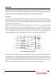
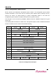
Device ID Register
Vendor ID
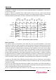
015
Table 2-6. Vendor ID Register Layout
Manufacturer of the device. The Valid ID is allocated by PCI SIG. If no specific vendor ID is assigned, the
14A1h value allocated by PCI SIG may be used. [RO : downloadable]
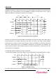
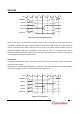
Device ID Register
15 0
Device ID
Table 2-7. Device ID Register Layout
A unique ID of each device. Device ID can be assigned by the manufacturer. [RO : downloadable]
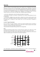
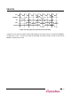
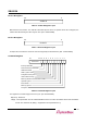
Command Register
Memory Space
9 1
Memory Write and Invalidate Enable
2
Parity Error Response
Fast Back-to Back Enable
8
VGA Palette Snoop
SERR# Enable
11
Wait Cycle Control
7
Special Cycles
10 6 4
I/O Space
Interrupt Disable
3
Reserved
5
Bus Master
015
Table 2-8. Command Register Layout
The register that controls reply for the PCI cycle. [non-downloadable]
Bit[15:11] : Reserved
Bit[10] : Interrupt Disable. The bit enables/disables INTX#. The value 0b enables INTX# and 1b disables
INTX#. The default is 0b. [R/W] (* Supported in PCI Specification 2.3)