SB4002A SB4002A PCI Intelligent Target Controller Ver 1.
SB4002A Contents 1. 2. 3. 4. 5. 6. 7. 8. 9. Introduction .............................................................................................................................. 6 PCI BUS .................................................................................................................................. 8 2.1 PCI Bus Protocol ................................................................................................................ 8 2.1.1 PCI Feature ........................
SB4002A Table of Contents Table 2-1. PCI Bus Signals ................................................................................................................................ 9 Table 2-2. PCI Bus Command ........................................................................................................................... 9 Table 2-3. PCI Bus I/O Addressing Rule .......................................................................................................... 10 Table 2-4.
SB4002A Table 3-2. WORD Data path Endian Conversion ............................................................................................ 46 Table 3-3. BYTE Data path Endian Conversion .............................................................................................. 47 Table 4-1. Serial ROM Address Map ............................................................................................................... 49 Table 6-1. Control Register Map .........................................
SB4002A Figure of Contents Figure 2-1. PCI BUS Basic Read Transaction ................................................................................................. 12 Figure 2-2. PCI BUS Basic Write Transaction ................................................................................................. 13 Figure 2-3. DEVSEL# timing............................................................................................................................ 13 Figure 2-4. Retry .......................
SB4002A 1. Introduction Summary of SB4002A features: Compliant with PCI Local Bus Specification 2.3 Supports 32-bit Bus / 33MHz and 66MHz Supports data transmission of max. 264MB/sec Supports PCI Power Management 1.
SB4002A acquired through SB4001, SB4002A offers more robustness and convenience than any other solutions. SB4002A will enable the users to develop the PCI target boards at reduced time and effort, and to replace the existing boards with cost-effective PCI option boards.
SB4002A 2. PCI BUS 2.1 PCI Bus Protocol 2.1.1 PCI Feature - PCI is a synchronous bus which supports 33MHz/66MHz clock and 32-bit/64-bit data path. (SB4002A supports 33MHz/66MHz clock and 32-bit data path.) PCI increases transmission efficiency via Linear/Cacheline wrap burst access. (SB4002A supports linear burst access.) PCI supports plug & play, and automatically reads the required resources from BIOS/OS and allocates them to the device.
SB4002A Signal name Type DEVSEL# s/t/s Device Select. Used by the selected target to indicate that it is selected. PERR# s/t/s Parity Error. Indicates that a parity error occurs in the data phase. SERR# o/d INTA#/INTB# INTC#/INTD# o/d Description System Error. Indicates occurrence of a critical error such as a parity error in the address phase. PCI interrupt signals. These signals except INTA# are the interrupt signals for multi functions. Table 2-1.
SB4002A Out of the commands mentioned in the above table, SB4002A does not support Interrupt Acknowledge, Special Cycle, Dual Address Cycle and the reserved commands. It does not support Memory Read Multiple, Memory Read Line, and Memory Write and Invalidate Command as well as SB4002A disregards the commands which are not supported. 2.1.4 PCI Addressing I/O Space Addressing In the I/O Address Space, all 32 AD lines(AD[31:0]) are used to provide a full byte address.
SB4002A Configuration Space of the intended target. Because SB4002A supports the single function only, only Function Number 0 is available. For accessing Configuration Space, SB4002A supports the IDSEL signal 1 only in the address phase. 2.1.5 PCI Basic Transaction All the functions specified below are based on the rising edge of CLK. Read Transaction All transactions are triggered as FRAME# is asserted. The bus master outputs the address on AD [31:0] and the command on C/BE [3:0]# as it asserts FRAME#.
SB4002A As Frame# is asserted, a burst access occurs. Because IRDY# is deasserted, a wait cycle is inserted by the master. At CLK 7, IRDY# is reasserted, and a data transfer occurs at CLK 8. At this point, because FRAME# is deasserted, the transaction is terminated. The master deasserts IRDY#, and the target deasserts TRDY# and DEVSEL#. Therefore a PCI BUS read transaction is completed.
SB4002A FRAME# is asserted, a burst access occurs. At CLK 4, IRDY# and TRDY# are asserted at the same time, and a data transfer occurs. As FRAME# is asserted, a burst access occurs. And as IRDY# and TRDY# are deasserted, a wait cycle is inserted. ADDRESS PHASE 1 DAT A PHASE 2 DAT A PHASE 3 4 DAT A PHASE 5 6 7 8 9 CLK FRAME# AD ADDRESS DATA- 1 DATA- 2 C/BE# BUS CMD BE#' s-1 BE#' s-2 DATA- 3 BE#' s-3 IRDY # TRDY # DEVS EL# Figure 2-2.
SB4002A device. The device sets the DEVSEL timing of status register of the configuration space header depending on the time point it can assert DEVSEL#. In the above figure, if DEVSEL# is asserted at CLK 2, CLK 3 and CLK 4, it is set to FAST (00b), MEDIUM (01b) and SLOW (10b), respectively. If no device has asserted DEVSEL# by CLK 4, the subtractive decoding device asserts DEVSEL#.
SB4002A that it cannot execute the transaction, it asserts STOP# instead of TRDY# at CLK 3. The master checks STOP# at CLK 4, and deasserts FRAME#. At CLK 5, the master deasserts IRDY#, and the target deasserts STOP# and DEVSEL#, terminating the transaction with RETRY, Disconnect The target terminates transaction when it cannot continue the burst from the master after it transfers at least one data signal.
SB4002A 1 2 3 4 5 6 7 CLK FRAME# IRDY# TRDY# STOP# DEVSEL# Figure 2-6. Disconnect Without Data In the above figure, a transaction is started at CLK 1, CLK 2 and CLK 3. If the burst access is unavailable at CLK 4, the target asserts STOP#3, indicating that it will disconnect. It also deasserts TRDY#, indicating that it will not transfer data any more. The master checks STOP# at CLK 5, deasserts FRAME#, and then, terminates the transaction at CLK 6.
SB4002A In the above figure, a transaction is started at CLK 1, CLK 2 and CLK 3. The target finds a critical error at CLK 4, deasserts TRDY# and DEVSEL#, and asserts STOP#. At CLK 5, the master checks this, recognizes Target-Abort, and deasserts FRAME#. At CLK 6, IRDY# and STOP# are deasserted, and the transaction is terminated with Target-Abort. 2.1.7 PCI Parity Generation & Checking In order to verify that address and data are transferred properly, PCI outputs the even parity signal via PAR.
SB4002A 1 2 3 4 5 6 7 8 9 CL K F RAME# AD ADDRESS DATA ADDRESS DATA PAR PERR# Figure 2-8. Parity Operation (First Read, Second Write) In figure 2-8, for read, the master checks PAR output by the target at CLK 5, and asserts PERR# if a parity error occurs. For write, the target checks PAR sent by the master at CLK 8, and asserts PERR# if a parity error occurs.
SB4002A 2.2 PCI Configuration Space Header All PCI devices must implement Configuration Space Header. The Configuration Space Header contains information on the device and the resources (base address space, interrupt, and etc.) used by the device. At system booting or system configuration, BIOS or OS reads the Configuration Space Header, runs P&P, and allocates the system resources. This I/O space can be accessed by DWORD, WORD and BYTE. SB4002A responses for type0 access only.
SB4002A Device ID Register 15 0 Vendor ID Table 2-6. Vendor ID Register Layout Manufacturer of the device. The Valid ID is allocated by PCI SIG. If no specific vendor ID is assigned, the 14A1h value allocated by PCI SIG may be used. [RO : downloadable] Device ID Register 15 0 Device ID Table 2-7. Device ID Register Layout A unique ID of each device. Device ID can be assigned by the manufacturer.
SB4002A Bit[9] : Fast Back-to-Back Enable. The bit indicates capability of fast back-to-back transaction between the master and other devices. This is activated when all the targets on the bus support fast backto-back transaction. The value 1b indicates that the master supports fast back-to-back transaction with other device, while 0b indicates that the master does not support fast back-toback transaction. Since this bit is for the master, SB4002A does not support this bit. The default is 0b.
SB4002A Status Register 15 14 13 12 11 10 9 8 7 6 5 4 3 2 0 Reserved Interrupt Status Capabilities Lis t 66 MHz Capable Reserved Fas t Back-to-Back Capable Data Parity Error Detected DEVSEL Tim ing Signaled Target Abort Received Target Abort Received Mas ter Abort Signaled Sys tem Error Detected Parity Error Table 2-9. Status Register Layout The status of the PCI bus of a device [downloadable] Bit[15] : Detect Parity Error. This bit is set if a parity error occurs in a device.
SB4002A SB4002A does not support this bit. The default is 0b. [RO] Bit[7] : Fast Back-to-Back Capable. The bit indicates whether the target device supports the fast back-toback transaction for a different device. 1b is support, and 0b is no-support. The default is 1b. [RO] Bit[6] : Reserved. The default is 0b Bit[5] : 66MHz Capable. The bit indicates whether the device supports 66MHz. 0b indicates that the device supports 33MHz only, and 1b indicates that the device supports both 33MHz and 66MHz.
SB4002A Cache Line Size Register 7 0 Cache Line Size Table 2-12. Cache Line Size Register Layout The register designates the size of the cache line of the system. Since this register is for the master, SB4002A does not support this register. The default is 0b. [RO : non-downloadable] Latency Timer Register 7 0 Latency Timer Table 2-13. Latency Timer Register Layout The register designates the latency clock for the bus master that executes a burst access.
SB4002A BIST(Built-in Self Test) Register 7 BIST Capable 6 Start BIST 5 4 Res erved 3 0 Completion Code Table 2-15. BIST Register Layout This register is used to control BIST. Bit[7] : The value 1b supports BIST, and 0b does not support BIST. Bit[6] : The value 1b starts BIST. When the BIST is finished, the device resets BIST by writing 0b on this bit. Bit[5:4] : Reserved. Bit[3:0] : The value 0b indicates that BIST is passed. Other values provide information on errors.
SB4002A For I/O Space 31 1 Bas e Addres s 0 1 Reserved I/O Space Indicator Table 2-17. Base Address Register for I/O space Bit[31:2] : This bit sets the base address of this I/O space. It is used by the address decoder. [W/R] Bit[1] : Reserved. [RO] Bit[0] : This bit indicates that Base Address Register maps I/O Space. [RO] Tips : How to set the Base Address Bit[31:4] of the memory base address and Bit[31:2] of the I/O base address are used to indicate the size and location of the I/O Space.
SB4002A Subsystem Vendor ID/Subsystem ID Register 15 0 Subs ys tem Vendor ID Table 2-18. Subsystem Vendor ID Register Layout 15 0 Subs ys tem ID Table 2-19. Subsystem ID Register Layout Subsystem ID shows information on the manufacturer and the subsystem. The register is used to identify the devices of the same vendor ID and the device ID. The vendor ID and the device ID provide information on the controller chip, and the subsystem vendor ID and the subsystem ID provide information on the PCI card.
SB4002A Interrupt Pin Register 7 0 Interrupt Pin Table 2-22. Interrupt Pin Register Layout This register indicates the PCI interrupt pin used by the device. Because SB4002A is a single function, the default value is set to 1h via INTA#. [RO : non-downloadable] MIN_GNT Register 7 0 MIN_GNT Table 2-23. MIN_GNT Register Layout This register indicates the time required for burst access. Because SB4002A does not support this register, the default is 00h.
SB4002A 2.3 PCI Power Management Interface In some cases, it is necessary to control the power supply of the PCI bus embedded system. Especially for the mobile system which uses an independent power supply or the PCI device which consumes a large amount of power, it is required to configure a low-power consuming system by limiting power supply when the PCI device is not is operation. The PCI specification defines the power management interface for easier power management.
SB4002A PMC(Power Management Capabilities) Register 15 11 10 9 8 6 5 4 3 2 PME_Support 0 Version D2_Support D1_Support Aux_Current DSI Reserved PME Clock Table 2-28. PMC Register Layout This register contains information on the power management capability of the device. [RO : nondownloadable] Bit[15:11] : PME Support. This bit shows the power state in which the device can assert PME#.
SB4002A PMCSR(Power Management Control/Status Register) 15 14 13 12 9 8 7 Data_Select 2 1 0 Reserved Power State PME_En Data_Scale PME_Status Table 2-29. PMCSR Layout This register controls power state and PME# of a device. [non-downloadable] Bit[15] : PME_Status. This bit is set to 1b if PME# is asserted. If this bit is 1b, the register is cleared and the PME# is deasserted. The default is 0b. [R/WC] Bit[14:13] : Data_Scale. This bit indicates the scale of the data register value. The default is 0b.
SB4002A PCI bus provides the PME# signal for Power Management Interface. PME# is used to request change of power state of a device. It is an open drain signal which is asynchronous to CLK. SB4002A provides the power management-related signal to the device in order to support the power management interface in efficient manner. SB4002A provides the input signal PME_REQ and the output signal PME_S. PME_REQ requests PCI bus to change the power state of the device, and PME_S shows the current power state.
SB4002A 2.4 Vital Product Data (VPD) VPD is a capability register prepared to provide additional information on the system and the device. VPD is located in the memory devices such as serial EEPROM. The data are accessed through the VPD capability register in the Configuration Space Header. The register addresses can be changed. In SB4002A, the register is in 48h~4Fh. In order to use VPD, you need to set the capability pointer to 48h. SB4002A adopts the VPD format defined in PCI Specification Revision 2.3.
SB4002A VPD Address Register 15 0 F VPD Address Table 2-34. VPD Address Register Layout Bit[15] F. This bit indicates that data transfer is finished between the VPD data register and the memory. For a read event, if 0b is written on F for the address, the device sets F when the data is prepared. The default is 0b. [R/W : non-downloadable] Bit[14:0] VPD Address. This bit indicates the address of VPD to be accessed by DWORD. The default is 00h.
SB4002A 2.5 CompactPCI Hot Swap CompactPCI is the specification made by applying the existing specification of PCI Local Bus for general PC to the industrial PC. The algorithms such as bus protocol are same as those of the existing PCI, except for the electrical features and the mechanical features. Hot Swap is one of the functions that reinforce the industrial aspect of CompactPCI. The function enables you to delete/insert the CompactPCI board while power is connected to the system.
SB4002A HS_CSR(Hot Swap Control and Status Register) 7 6 INS EXT 5 4 PI 3 2 1 0 LOO PIE EIM DHA Table 2-39. HS_CSR Layout The register enables the host to adjust the hot swap process. [non-downloadable] Bit[7] : INS. ENUM# Status - Insertion. This bit indicates that ENUM# is asserted during the insert process. If the value is 1b, the bit is cleared and ENUM# is deasserted. The default is 0b. [R/WC] Bit[6] : EXT. ENUM# Status - Ejection.
SB4002A 2.6 Exclusive Access PCI bus provides the method that the master can exclusively access a specific target. This method is called an exclusive access. It is started by LOCK#, one of the PCI signals. The first transaction to start an excusive access for a specific target must be the memory READ transaction. If this transaction is started, LOCK# must be deasserted at the first CLK of the address phase, and LOCK# must be deasserted at the next CLK.
SB4002A In the above figure, FRAME# is asserted at CLK 2 and the address phase is started. As LOCK# is asserted, if the PCI command is Memory Read, the exclusive access request transaction is executed. As LOCK# is asserted at CLK 3 and the data phase is terminated normally at CLK 4, an exclusive access is started. 1 2 3 4 5 CLK FRAME# Release LOCK# Continue AD ADDRESS DATA IRDY# TRDY# DEVSEL# Figure 2-10.
SB4002A 3. Legacy Bus SB4002A provides the ISA like Legacy bus at the back end, in order that it can interface with general devices via interworking with PCI bus. SB4002A provides the chip select signal (CSx#), I/O read/write(IOR#, IOW#) and memory read/write#(MEMR#, MEMW#) signal to support the general devices. SB4002A also supports a variety of flexible accessing methods. 3.1 Real Access/Delayed Access 3.1.
SB4002A 3.1.2 Delayed Access This method transmits data through the transaction on the Legacy bus after the device completes the transaction on the PCI bus. If the timing of the device is slow or the burst size is too big, data transfer in the real access method may seize the PCI bus for a long time, and deteriorate the overall system efficiency.
SB4002A CLK AD FRAME# IRDY# DEVSEL# TRDY# STOP# EA ED CS# IOR# Figure 3-3. Legacy Bus Delayed Read Access 3.2 Single Access/Burst Access Single and burst access on the Legacy bus are the signal access / burst access on the PCI bus. In other words, the single read/write on the PCI bus is transmitted to the single read/write on the Legacy bus, and the burst read/write on the PCI bus is transmitted to the burst read/write on the Legacy bus.
SB4002A CLK AD FRAME# IRDY# DEVSEL# TRDY# EA ED CS# IOR# Figure 3-5. Legacy Bus Real Read Burst Access CLK AD FRAME# IRDY# DEVSEL# TRDY# EA ED CS# IOW# Figure 3-6.
SB4002A CLK AD FRAME# IRDY# DEVSEL# TRDY# STOP# EA ED CS# IOR# Figure 3-7. Legacy Bus Delayed Read Burst Access Single and burst in a delayed access are depending on whether it is a write access or a read access. In case of a delayed write access, a burst access is executed on the PCI bus, and the data are stored in the FIFO memory. (Maximum 16 bytes. If the access request exceeds the limit, the device terminates the transaction with disconnect.
SB4002A 3.3 Data Split and Combine SB4002A supports the data path in BYTE, WORD and DWORD on the Legacy bus depending on the characteristics of the device. The PCI bus data path is based on DWORD, and access in byte and word is also available. If the supported data path type is not consistent between the PCI bus access and the Legacy bus device - e.g.
SB4002A CLK AD C/BE# 0000 0000 FRAME# IRDY# DEVSEL# TRDY# STOP# EA ADD ADD+1 ADD+2 ADD+3 ED[7:0] CS# IOR# Figure 3-9.
SB4002A 3.4 Endian Conversion The data are divided into Little Endian and Big Endian depending on the order or BYTE lanes in the system structure. In case of a DWORD system with the [31:0] data path, in Little Endian, [31:24], [23:16], [15:8] and [7:0] are the fourth, third, second and first byte, respectively. In Big Endian, [7:0], [15:8] and [23:16] are the fourth, third and fourth byte, respectively. Basically, PCI bus is based on Little Endian.
SB4002A - BYTE Data path Byte Lane Little Endian PCI bus Little Endian Lagacy bus Big Endian Lagacy bus BYTE3 BYTE2 BYTE2 BYTE0 AD[31:24] AD[23:16] AD[15:8] AD[7:0] ED[7:0] ED[7:0] ED[7:0] ED[7:0] ED[7:0] ED[7:0] ED[7:0] ED[7:0] Table 3-3.
SB4002A 4. Configuration Data in Serial ROM The PCI Configuration Space Header is an important part of the PCI bus. The Header contains information on the product and the resources, which is a unique value for each product. Because the Header must contain unique information by product, SB4002A reads out information from the external serial ROM. SystemBase adopts ATMEL's 1K 3-wire Serial EEPROM AT93C46 as the external ROM. Any other ROM which is equivalent to AT93C46 can be used.
SB4002A Address Description 15h Base Address3 2nd byte 16h Base Address3 3rd byte 17h Base Address3 4th byte 18h Base Address4 1st byte 19h Base Address4 2nd byte 1Ah Base Address4 3rd byte 1Bh Base Address4 4th byte 1Ch Base Address5/Base Address0 1st byte 1Dh Base Address5/Base Address0 2nd byte 1Eh Base Address5/Base Address0 3rd byte 1Fh Base Address5/Base Address0 4th byte 20h Subvendor ID Low byte 21h Subvendor ID High byte 22h Subsystem ID Low byte 23h Subsystem ID High
SB4002A 00h~2Fh of the serial ROM are used to set the PCI Configuration Space Header. At the system reset, the device automatically reads this part from the serial ROM and sets the Configuration Space Header. You can use 30h~7Fh at your own discreet. Because you can read/write data through the serial ROM interface register in the control register, you can easily store data without seizing other resources.
SB4002A Serial ROM Address (06h) : Status Register Capabilities List Enable The PCI spec from 2.1 provides a new register set which is a linked list called as the Capabilities List. In order to enable the Capabilities List, the Capabilities List bit (bit 4) of the PCI Status Register must be set to 1, and the Capabilities List pointer must be in the PCI Configuration Space 34h. In 34h, the pointer indicates the first item of the Capabilities List.
SB4002A Serial ROM Address(0Eh) : Base Address1 3rd Byte Serial ROM Address 0Eh represents the third bit array [23:16] of Base Address1[31:0] in PCI Configuration Space 14h~17h. Serial ROM Address(0Fh) : Base Address1 4th Byte Serial ROM Address 0Fh represents the fourth bit array [31:24] of Base Address1[31:0] in PCI Configuration Space 14h~17h.
SB4002A Serial ROM Address(17h) : Base Address3 4th Byte Serial ROM Address 17h represents the fourth bit array [31:24] of Base Address3[31:0] in PCI Configuration Space 1Ch~1Fh. Serial ROM Address(18h) : Base Address4 1st Byte Serial ROM Address 18h represents the first bit array [7:0] of Base Address4[31:0] in PCI Configuration Space 20h~23h.
SB4002A Serial ROM Address(1Eh) : Base Address5/Base Address0 3rd Byte If the Control Register Setting0 byte of the Serial ROM Address 00h is 00h, Serial ROM Address (1Eh) represents the bit array [23:16] of Base Address5[31:0] in PCI Configuration Space 24h~27h. If the Control Register Setting0 byte of the Serial ROM Address 00h is 01h, Serial ROM Address (1Eh) represents the bit array [23:16] of Base Address0[31:0] in PCI Configuration Space 10h~13h.
SB4002A Serial ROM Address(25h) : EXROM Base Address 2nd Byte Serial ROM Address(25h) represents the bit array [15:8] of Expansion ROM Base Address[31:0] of PCI Configuration Space 30h~33h. Serial ROM Address(26h) : EXROM Base Address 3rd Byte Serial ROM Address(26h) represents the bit array [23:16] of Expansion ROM Base Address[31:0] of PCI Configuration Space 30h~33h.
SB4002A If you want to use the VPD Capability only, store 48h and 00h in 34h and 49h, respectively, of the PCI Configuration Space. If you want to use the CompactPCI Hot Swap Capability only, store 50h in 34h of the PCI Configuration Space. If 00h is stored in 34h of the PCI Configuration Space, the three Capabilities are disabled. Serial ROM Address(29h) : NEXT PTR0 Serial ROM Address(29h) represents the Next Item Pointer of PCI Power Management Interface Capability List.
SB4002A The Data Register is located in 47h of the PCI Configuration Space. (See 2.3 PCI Power Management Interface for further details.) Serial ROM Address(2Dh) : PMC Data 4 Serial ROM Address(2Dh) is used to specify the reading value from Data Register in case Data Select bits(PMCSE[12:9]) of PMCSR equal to 4h. In other words, it indicates the D0 State Power Dissipated. The Data Register is located in 47h of the PCI Configuration Space. (See 2.3 PCI Power Management Interface for further details.
SB4002A 5. Miscellaneous Feature 5.1 Interrupt In order to enable the PCI interrupt service, SB4002A provides 5 interrupt pins to the Legacy bus. In general, the I/O devices use the interrupt and provide total 5 base addresses, SB4002A provides 5 interrupt pin sources. However, the interrupt pins can be used regardless of the address. For example, an I/O base address can use 2 or more interrupt pins.
SB4002A 5.2 General Purpose I/O Interface SB4002A provides total 8 GPIO ports. In order to control the 8 GPIO ports, SB4002A also provides GPIO Output Enable Register, GPIO Output Register and GPIO Input Register. GPIO Out Enable Register GPIOn (n = 0, 1, 2, ... , 7) GPIO Output Register GPIO Input Register Figure 5-2. GPIO Controller Schematic 5.3 Serial ROM Interface In order to import the configuration data, SB4002A provides an external serial EEPROM.
SB4002A 6. Control Register Theses addresses are used to define various internal selections and to implement the supplementary functions. The Control Register Setting0/1(See 4. Configuration Data in Serial ROM)of the Serial ROM allocates the Base Address0 or the Base Address5 to I/O Space or Memory Space in the PCI Configuration Space Header, and supports access to the unit of DWORD. The table below describes the details of the Control Registers.
SB4002A BASE ADDRESS1/2/3/4/5 & EXPANSION ROM BASE Address Space Setting Register 31 26 25 24 23 22 Reserved R 20 19 18 16 15 14 12 11 10 8 7 6 R R R R R = Reserved 4 3 2 1 0 Data Path RD# to RD# Langth RD# Length WR# to WR# Length WR# Length Prefetch Length Read Mode Write Mode Table 6-2. Base Address Space Setting Register If burst access is requested for the device which does not support burst access, the device finishes the cycle with Disconnect.
SB4002A Bit[10:8] : WR# Adding Length for Legacy Bus (R/W) Basically, IOW# has the enable length of PCI 1 CLK. The length is extended by the value set in this value. This bit is used to control the wait cycle on the PCI bus in the real time write. Bit[6:5] : READ Prefetch Byte (R/W) Supported in the delay time read mode only.
SB4002A Legacy bus. The device deasserts TRDY# at the next CLK, asserts IOW# on the Legacy bus, and outputs the data. Then, the above procedure is repeated. Therefore, the TRDY# to TRDY# wait cycle on the PCI bus is bit[9:7]+bit[15:13]+10b. 2. Delayed Time Write In a single transfer, when DEVSEL# is asserted, TRDY# is asserted at the same time to catch the data, and the device ends the PCI cycle. After an appropriate time period, the device asserts CS# and approves the address and data.
SB4002A If a new read cycle is started after retry, the previous cycle is disregarded. If a PCI cycle is started when a read cycle on the Legacy bus is not finished, the device ends the cycle with retry. 5. Delayed Time Read with Prefetch It is applied to a burst transfer only. On receiving the initial access, the device stores the address and command, finishes the PCI bus cycle with retry, and after an appropriate time period, executes a read transaction on the Legacy bus.
SB4002A Reset Register 7 0 SW RESET Table 6-3. Reset Register Layout This register resets the chip internal register and Legacy bus in the software level. (Write Only) Bit[7:0] : If 52h corresponding to “R" is used, the default is the chip internal register (excluding the register on Configuration Space Header and Reset Register), and the reset signal is output through the reset pin on the Legacy bus. If other values are used, reset is released.
SB4002A GPIO Output Register 7 6 5 4 3 2 R GO6 GO5 GO4 GO3 GO2 R = Reserved 1 0 GO1 GO0 Table 6-5. GPIO Output Register Layout Sets output of each GPIO. Bit[7] : Reserved Bit[6] : GO6, Sets the output of GPIO6. Bit[5] : GO5, Sets the output of GPIO5. Bit[4] : GO4, Sets the output of GPIO4. Bit[3] : GO3, Sets the output of GPIO3. Bit[2] : GO2, Sets the output of GPIO2. Bit[1] : GO1, Sets the output of GPIO1. Bit[0] : GO0, Sets the output of GPIO0.
SB4002A Interrupt Enable Register 7 5 Reserved 4 3 2 1 0 IE4 IE3 IE2 IE1 IE0 Table 6-7. Interrupt Enable Register Layout Enables/Disables 5 interrupt signals. (R/W) Bit[4] : IE4, 1b : Enables INT5, 0b : Disables INT5(Default). Bit[3] : IE3, 1b : Enables INT4, 0b : Disables INT4(Default). Bit[2] : IE2, 1b : Enables INT3, 0b : Disables INT3(Default). Bit[1] : IE1, 1b : Enables INT2, 0b : Disables INT2(Default). Bit[0] : IE0, 1b : Enables INT1, 0b : Disables INT1(Default).
SB4002A Poll Register 7 5 Reserved 4 3 2 1 0 POL4 POL3 POL2 POL1 POL0 Table 6-9. Poll Register Layout Indicates the interrupt status on the Legacy bus regardless of the enable register value. Bit[4] : POL4, 1 : Indicates generation of an INT5. Bit[3] : POL3, 1 : Indicates generation of an INT4. Bit[2] : POL2, 1 : Indicates generation of an INT3. Bit[1] : POL1, 1 : Indicates generation of an INT2. Bit[0] : POL0, 1 : Indicates generation of an INT1.
SB4002A Muxed Pin Control Register R = Reserved 15 14 13 12 11 10 9 8 7 6 5 4 3 2 1 0 R R INT5/GPIO4 INT4/GPIO3 INT3/GPIO2 INT2/GPIO1 INT1/GPIO0 EA23/GPIO7 EA24/GPIO6 EA25/GPIO5 EA26/CSX# EA27/CS5# EA28/CS4# EA29/CS3# EA30/CS2# EA31/CS1# Table 6-11. Muxed Pin Control Register Layout Sets the values for other supplementary functions.
SB4002A 70
SB4002A 7. Physical Specification RSK VCC VSS RDI RDO 91 90 89 RCS 94 92 HLED 95 93 VSS 96 BE3# PME_REQ 100 HSW ED31 101 VCC ED30 102 97 ED29 103 PME_S ED28 104 98 VSS 105 99 VCC 106 OPCLK ED27 ED23 113 107 ED22 114 ED26 ED21 115 108 VSS 116 ED25 VCC 117 109 ED20 118 110 ED19 119 BE2# ED18 120 ED24 ED17 121 111 ED16 122 112 VSS 123 ED15 127 124 ED14 128 BE1# ED13 129 VCC ED12 130 125 ED11 131 126 ED10 132 7.
SB4002A 7.2 Pin Description Signal Pin Pin Name No. Type Description PCI Bus Signal Provides timing for all actions of PCI bus. The signal gives input for all CLK 33 in PCI the PCI devices, and its rising edge becomes the reference for input/output and timing constant of all signals. (exception: RST#, INTx#, PME#, CLKRUN# ) PRST# 32 in PCI Reset signal of the PCI system. Address/Data multiplexed signal.
SB4002A Signal Pin Pin Name No. Type INTA# 31 Description o/d PCI interrupt signal. PME# 34 o/d Power Management Event. Requests change of power state of a device or a system. Enabled when the power management interface capability is supported. ENUM# 88 o/d Enumeration. Shows that the board has been inserted to the system, or is about to be removed. This is enabled when the CompactPCI Hot Swap is supported.
SB4002A Signal Pin Pin Name No. Type IOW# 148 out I/O Write Signal. Asserted at write access in the I/O port. MEMR# 153 out Memory Read Signal. Asserted at read access in the memory. MEMW# 152 out Memory Write Signal. Asserted at write access in the memory. out Byte Enable Signal. Enable signal for each byte of the data signal on the Legacy bus. BE[3]#,BE[2]#,BE[1]#,BE[0]# are corresponding to ED[31:24], ED[23:16], ED[15:8] and ED[7:0], respectively.
SB4002A Signal Pin Pin Name No. Type Description Others TMD 23 in Connected to VCC via the 10K resistance. NC 21 22 - No Connection Table 7-1.
SB4002A 7.3 Package Dimension THIN QUAD FLATPACK 0,23 0,13 0,10 0,4 1,20 MAX 1,05 0,95 17,2 20,0 22,0 NOTES: A. All linear dimensions are in millimeters. B. This drawing is subject to change without notice.
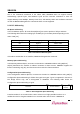
SB4002A 7.3 Electrical Specification SB4002A is based on 3.3V I/O, and supports 5V tolerance. Recommended Operation Conditions Parameters Minimum Maximum Power Supply 3.0V 3.6V PCI input -0.5V 0.3xVDD General input -0.5V 0.3xVDD PCI input 0.5xVDD 5.5V General input 0.7xVDD 5.5V Operating Temperature -40℃ 85℃ Storage Temperature -40℃ 150℃ Conditions VIL,low level input voltage Guaranteed Input Low Voltage VIH,low level input voltage Guaranteed Input High Voltage Table 7-2.
SB4002A 78
SB4002A 8. Timing Specification 8.
SB4002A V_Th CLK V_test V_Tl T_val OUTPUT DELAY V_tfall T_val OUTPUT DELAY V_trise Tri-State OUTPUT T_on T_off Figure 8-1. Output Timing Measurement Conditions V_Th CLK V_test T_su V_Tl T_h V_Th INPUT V_test inputs valid V_test V_max V_Tl Figure 8-2. Input Timing Measurement Conditions * PCI Bus timing specification is as defined in the PCI Local Bus Specification Ver 2.3. * SB4002A satisfies the above mentioned timing specification in the aspect of PCI Bus interface.
SB4002A 8.2 Legacy Bus Timing Specifications Symbol Parameter CS#/EA/BYTE_EN# assert to Td1 IOW#/MEMW# assert IOW#/MEMW# deassrt to Td2 CS#/EA/BYTE_EN# deassert Min Typ Max - 1 - - 1 - Td3 IOW#/MEMW# enable to ED valid - - 3 Td4 IOW#/MEMW# disable to ED valid - 1 - Tw1 IOW#/MEMW# width - n - * ‘n’ meams IOW#/MEMW# signal width is ‘n’ times PCI CLK. ‘n’ would be determined by Base Address Space Setting Register[10:8], Refer to Chapter 6 Table 8-2.
SB4002A Symbol Parameter CS#/EA/BYTE_EN# assert to Td5 IOR#/MEMR# assert IOR#/MEMR# deassrt to Td6 CS#/EA/BYTE_EN# deassert ED valid to IOR#/MEMR# disable (required setup time for read on 66MHz) Trs ED valid to IOR#/MEMR# disable (required setup time for read on 33MHz) IOR#/MEMR# disable to ED unvalid Trh (reguired hold time for read) Tr1 IOR#/MEMR# width Min Typ Max - 1 - - 1 - 15.5 - - 19.
SB4002A 9. Company Information SystemBase Co., Ltd.