
SB16C1058PCI_Data Sheet_EN

SB16C1058PCI
PCI Target Interface Controller
with Octal-UART
JULY 2013 REV 1.04
14
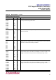
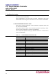
Table 6–1: Pin Description…continued
Name
Pin
Type
Description
C/BE[3]#
C/BE[2]#
C/BE[1]#
C/BE[0]#
63
73
95
106
T/S
T/S
T/S
T/S
Bus Command and Byte Enables: These signals are multiplexed on same
pins. During the address phase of transaction, C/BE[3:0]# define the bus
command. During the data phase, C/BE[3:0]# are used as Byte Enables.
PAR
84
T/S
Parity: Parity is even parity across AD[31:00] and C/BE[3:0]#.
FRAME#
74
S/T/S
Cycle Frame: This signal is driven by the master of main system to indicate
the beginning and duration of an access.
IRDY#
77
S/T/S
Initiator Ready: This signal indicates the initiating agent’s(main system’s)
ability to complete the current data phase of the transaction.
TRDY#
78
S/T/S
Target Ready: This signal indicates the target agent’s(SB16C1058PCI’s)
ability to complete the current data phase of the transaction.
STOP#
80
S/T/S
Stop: This signal indicates that the current target(SB16C1058PCI) is
requesting the master to stop current transaction.
LOCK#
81
S/T/S
Lock: This signal provides for exclusive use of a resource. SB16C1058PCI
may be locked by one master at a time. See the PCI Local Bus Specification
for the detail operation of lock function.
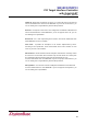
IDSEL
64
I
Initialization Device Select: This is used for chip selection during
configuration read and write transaction.
DEVSEL#
79
S/T/S
Device Select: This signal indicates that the driving device has decoded its
address as the target of the current access. As an input, DEVSEL# indicates
whether any device on the bus has been selected.
PERR#
82
S/T/S
Parity Error: This signal is only for reporting data parity errors during all PCI
transactions except Special Cycle.
SERR#
83
S/T/S
System Error: This signal is for reporting address parity errors, data parity
errors on the Special Cycle command, or any other system error where the
result will be catastrophic.
PCI_33M#
126
I
PCI Operational Speed: This input is for selecting the operational speed of
PCI Bus. This chip is operated at 33MHz PCI Bus when this pin is cleared to
0b. And it is operated at 66MHz PCI Bus when this pin is setted to 1b.
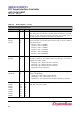
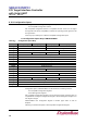
Other Interfaces
Name
Pin
Type
Description
XIN
118
I
Crystal or External Clock Input: This input of up to 85MHz for data rate of
5.3Mbps at 3.3V.
XOUT
117
O
Crystal or Buffed Clock Output: This output level is 3.3V.
WAKE_REQ
149
I
WAKE Request: PM state of PCI Device goes from D3 state to D0 state with
the Wake Up Event. This pin receives the event signal needed for the
transition from D3 state to D0 state.
PME_S
170
O
PME Status: This signal indicates PM state. If PM state is in D0 state, it is set
to 1b and if PM state is in D3 state, it is cleared to 0b.