
SB16C1054PCI_Data Sheet_EN

SB16C1054PCI
PCI Target Interface Controller
with Quad-UART
JULY 2013 REV 1.04
27
9.2.2 SB16C1054PCI Power Management Wakeup implementation
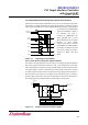
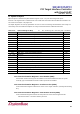
Below figure is Logic Diagram of MAX3243. As you can see from this figure, RIN2 input
signal (this pin is mainly prepared to be used by Ring Indicator.) is forked to reversed
output signal called ROUT2 and output called ROUT2B. Among these, ROUT2B signal
is not influenced by FORCEOFF#
signal and input/output of buffer is
not restricted. RIn input is
screened by FORCEOFF# but
above ROUT2B logic is Open
when FORCEOFF# so RIn signal
becomes an input without
reversion. This signal is connected
to WAKEREQ of SB16C1054PCI
and handled as Wake Event. And
if it is in D3
cold
state, this signal is
asserted as PME# side band
signal.
Figure 9–2: Logic Diagram of MAX3243
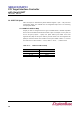
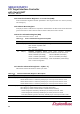
9.2.3 3.3Vaux Presence Detection & Power Routing
PCI Add-In Card that implements a function which can generate Power Management
Event from D3cold must decide existence of 3.3V on Pin B10(3.3Vaux) of PCI Bus.
When weak pull-down attached to Pin B10 is implemented on system board that does
not support supply of 3.3Vaux, it should be there to make logic low reference and must
be implemented in all Add-In Card. On systems that do not supply 3.3Vaux through Pin
B10, PCI Add-In Card must use any voltage source that Add-In Card can supply to
provide supply to Aux Power of its own. So depending on existence of 3.3Vaux of Pin
B10, design a circuit that supplies Power to its Aux Power as shown above.
Figure 9–3: Sample Circuit for Aux Power Supply
FORCEOFF#
RIN3ROUT3
ROUT5
FORCEON
ROUT1
RIN4
RIN5
ROUT2
ROUT2B
RIN1
Auto-power down
RIN2
ROUT4
3.3Vaux (IN2) > +3.3V (IN1)
3.3Vaux
+3.3V
R4
10K
A14
Yes
VSNS > 0.8V
B19
No
Add-in Card_Vaux (OUT)
C2
22uF
C1
22uF
X
Presence Detect
R1
2.5K 1%
+3.3V
No
R2
1K 1%
Add-in Card_Vaux
(to auxiliary power
plane)
+3.3V
U1
TPS2113A
1
2
3
4 5
6
78
STAT
EN
VSNS
ILIM GND
IN2
OUTIN1
A16
R3
400R
No
Yes 3.3Vaux
+3.3V
PCI
Connector
Pinout
A10+3.3V