SB16C1054PCI PCI Target Interface Controller with Quad-UART JULY 2013 REV 1.04 PCI Target Interface Controller SB16C1054PCI Revision 1.04 SystemBase Co., Ltd.
SB16C1054PCI PCI Target Interface Controller with Quad-UART JULY 2013 REV 1.04 CONTENTS 1. Description ................................................................................................................................................. 5 2. Features ..................................................................................................................................................... 5 2.1 PCI Interface .............................................................................
SB16C1054PCI PCI Target Interface Controller with Quad-UART JULY 2013 REV 1.04 9. Power Management ................................................................................................................................ 25 9.1 PCI Power Management ................................................................................................................ 25 9.1.1 PCI Function Power State .................................................................................................... 25 9.
SB16C1054PCI PCI Target Interface Controller with Quad-UART JULY 2013 REV 1.04 13.1 Transmit Holding Register (THR, Page 0) .................................................................................... 50 13.2 Receive Buffer Register (RBR, Page 0) ....................................................................................... 50 13.3 Interrupt Enable Register (IER, Page 0) ...................................................................................... 51 13.
SB16C1054PCI PCI Target Interface Controller with Quad-UART JULY 2013 REV 1.04 1. Description SB16C1054PCI is a PCI Target Interface Controller with Quad-UART. It offers easy PCI Target Card Adapter implementation. SB16C1054PCI provides high performance serial communication. With a built-in four SB16C1050 Cores that have built-in 256-byte FIFO, SB16C1054PCI decreases CPU load, is stronger at errors such as Overrun error and works well with simultaneous use of multiple ports.
SB16C1054PCI PCI Target Interface Controller with Quad-UART JULY 2013 REV 1.04 ■ Software Selectable Baud Rate Generator ■ Prescaler Provides Additional Divide-by-4 Function ■ Programmable Sleep Mode ■ Programmable Serial Interface Characteristics - 5, 6, 7, or 8-bit Characters - Even, Odd, or No Parity Bit Generation and Detection - 1, 1.
SB16C1054PCI PCI Target Interface Controller with Quad-UART JULY 2013 REV 1.04 4.
SB16C1054PCI PCI Target Interface Controller with Quad-UART JULY 2013 REV 1.04 5. Applications 5.1 Serial 4-port Serial 4-port Card is generally made with SB16C1054PCI. Special logic is not needed to make one serial port since quad-UART are built inside the SB16C1054PCI. SB16C1054PCI is the best and cost effective one-chip solution for 4-port serial card application. Users can make a serial application with RS232, RS422 or RS485 transceivers easily.
SB16C1054PCI PCI Target Interface Controller with Quad-UART JULY 2013 REV 1.04 6.
SB16C1054PCI PCI Target Interface Controller with Quad-UART JULY 2013 REV 1.04 Table 6–1: Pin Description Modem and Serial I/O Interface Name Pin Type Description TXD0 23 O Transmit Data: These pins are individual transmit data output. During the TXD1 TXD2 13 1 O O local loop-back mode, the TXD output pin is disabled and TXD data is internally connected to the RXD input. TXD3 130 O RXD0 26 I Receive Data: These pins are individual receive data input.
SB16C1054PCI PCI Target Interface Controller with Quad-UART JULY 2013 Table 6–1: REV 1.04 Pin Description…continued Function Configuration Interfaces Name Pin Type Description ALL_EN 107 I ALL Enable: When this pin is set, each port can be selected CLKSEL 95 I RS232, RS422 or RS485 interface per port. Clock Select: This pin selects the divide-by-1 or divide-by-4 prescalable clock. During the reset, The high on CLKSEL selects the divide-by-1 prescaler.
SB16C1054PCI PCI Target Interface Controller with Quad-UART JULY 2013 REV 1.04 Table 6–1: Pin Description…continued Function Configuration Interfaces Name Pin Type Description INTF2[1] INTF2[0] 113 114 I I Line Interface Type Select for 3’rd Port: When ALL_EN = 1b in Serial 4-port Mode, these pins are used to select the type of line transceiver in 3’rd serial port. The inputted value from these pins is shown in IIR1[5:4] of the Option register.
SB16C1054PCI PCI Target Interface Controller with Quad-UART JULY 2013 Table 6–1: REV 1.04 Pin Description…continued PCI Interfaces Name Pin Type Description CLK 37 I PCI Clock: PCI clock provides timing for all transaction on SB16C1054PCI. RESET# 39 I PCI Reset: Reset the SB16C1054PCI. The inputted signal indicates when the applied main power is within the specified tolerance and stable. This signal is asynchronous to CLK when asserted or deasserted.
SB16C1054PCI PCI Target Interface Controller with Quad-UART JULY 2013 Table 6–1: REV 1.04 Pin Description…continued Name Pin Type Description TRDY# 66 S/T/S Target Ready: This signal indicates the target agent’s(SB16C1054PCI’s) ability to complete the current data phase of the transaction. STOP# 68 S/T/S Stop: This signal indicates that the current target(SB16C1054PCI) is LOCK# 69 S/T/S requesting the master to stop current transaction.
SB16C1054PCI PCI Target Interface Controller with Quad-UART JULY 2013 Table 6–1: REV 1.04 Pin Description…continued Power and Ground Name Pin Type Description VCC 9, 27, 46, 64, 82, 100, 117, PWR Power Supply: Connect to +3.3V and to Core Ground through 135 GND 10, 28, 45, 63, 81, 96, 99, 0.1uF capacitors. GND Ground: Connect to ground. I Reserved for Test: Used for SB16C1054PCI internal testing. 118, 136 RSVD 101 Must be wired to VCC via the 10K resistance.
SB16C1054PCI PCI Target Interface Controller with Quad-UART JULY 2013 REV 1.04 7. Configuration Loader SB16C1054PCI can perform system initialization by reading PCI Configuration header data from external serial EEPROM. When SB16C1054PCI is reset after power is granted, Configuration Loader inside SB16C1054PCI loads Configuration header data and etc from external serial EEPROM. 7.
SB16C1054PCI PCI Target Interface Controller with Quad-UART JULY 2013 REV 1.04 Vendor ID : Represents manufacturer of device. It is a unique ID given by PCI SIG and must be downloaded from external serial EEPROM. If you do not own Vendor ID, you can use 14A1h given to SystemBase by PCI SIG with permission. Device ID : A unique ID of each device and is assigned at manufacturer’s discretion and must be downloaded from serial EEPROM. If you do not prepare Device ID, you can use 0004h given to SystemBase.
SB16C1054PCI PCI Target Interface Controller with Quad-UART JULY 2013 REV 1.04 8. PCI Configuration Space PCI Configuration offers one type of Configuration Space access method. - PCI Compatible Configuration method PCI Compatible Configuration method is compatible with PCI version 2.3 and higher and supports 100% binary compatibility to software for operating system agreed bus list and organization. From 0 byte up to 256 bytes is called PCI Compatible Configuration Space 8.
SB16C1054PCI PCI Target Interface Controller with Quad-UART JULY 2013 REV 1.04 8.1.1 Vendor ID A 16-bit register which represents the manufacturer of the device. It is a unique ID given by PCI SIG after membership registration and must be downloaded from external serial EEPROM. If you do not own a Vendor ID, it is fine to use 14A1h given to SystemBase by PCI SIG. 8.1.
SB16C1054PCI PCI Target Interface Controller with Quad-UART JULY 2013 REV 1.04 8.1.4 Status Register Table 8–3: Status Register Bit Type 15 RW 14 RW 13 RW Description Detected Parity Error: This bit must be set by the device whenever it detects a parity error, even if parity error handling is disabled. Default value of this bit is 0b. Signaled System Error: This bit must be set whenever the device asserts SERR#. Devices that will never assert SERR# do not need to implement this bit.
SB16C1054PCI PCI Target Interface Controller with Quad-UART JULY 2013 REV 1.04 8.1.5 Revision This register shows device revision. Manufacturer can assign it freely and must be downloaded from serial EEPROM. If you do not prepare Revision ID, you can use B0h given to SystemBase. It is also related to software device driver installation. 8.1.6 Class Code This register contains descriptions on functions the device implements and must be downloaded from serial EEPROM.
SB16C1054PCI PCI Target Interface Controller with Quad-UART JULY 2013 REV 1.04 8.1.11 Base Address Registers These are spaces for assigning Base address for accessing I/O device or memory on PCI Local Bus. There are 6 spaces from Base Address Register 0 to 5, but spaces from Base Address Register 2 to 5 are set as unused reserved area. In SB16C1054PCI, Base Address Register 0 is used for UART and Base Address Register 1 is used for Option Registers.
SB16C1054PCI PCI Target Interface Controller with Quad-UART JULY 2013 REV 1.04 8.2 Power Management Registers of SB16C1054PCI Sometimes control over power is needed on PCI Bus applied systems. Especially in cases when system uses independent power source like mobile system or when PCI device uses a lot of power, the system must limit power supply to PCI device when it is not in use to make a power efficient system.
SB16C1054PCI PCI Target Interface Controller with Quad-UART JULY 2013 REV 1.04 8.2.4 Power Management Control/Status Register (44~45h) This 16bit Register manages PCI Function’s Power Management state and it is also used to enable and monitor PME. Table 8–8: Power Management Control/Status Register Bit Type Description 15 RW PME_Status: This bit is set when the function would assert the PME# signal independent of the state of the PME_En bit.
SB16C1054PCI PCI Target Interface Controller with Quad-UART JULY 2013 REV 1.04 9. Power Management PCI was the most famous and useful bus since it was introduced in 1992. It is used in various computer systems from Laptops to Servers. It supported high performance applications by offering large bandwidth and efficiently supporting multiple masters. Also, it offers efficient power management through Power Management and various types of Form Factor modules and Applications.
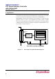
SB16C1054PCI PCI Target Interface Controller with Quad-UART JULY 2013 REV 1.04 Power On Reset D0 Uninitialized PCI RST# Sof t Reset D0 Active D2 D3cold D1 Figure 9–1: D3 hot Vcc Remov ed PCI Function Power Management State Transition Cf. Hibernate state is variation of shutdown state. In this state, all states of computer is saved on disk and thus when power comes back, it can be started as current session. 9.2 SB16C1054PCI Power Management Pins and Functions 9.2.
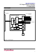
SB16C1054PCI PCI Target Interface Controller with Quad-UART JULY 2013 REV 1.04 9.2.2 SB16C1054PCI Power Management Wakeup implementation Below figure is Logic Diagram of MAX3243. As you can see from this figure, RIN2 input signal (this pin is mainly prepared to be used by Ring Indicator.) is forked to reversed output signal called ROUT2 and output called ROUT2B.
SB16C1054PCI PCI Target Interface Controller with Quad-UART JULY 2013 REV 1.04 10. UART I/O Space UART I/O Space is determined by Base Address Register 0 (10h ~ 13h) from PCI Configuration Space. This is BAR0 area of Configuration Space and is for accessing actual physical UARTs. 10.1 UART I/O Address Map 8 bytes per Port are assigned since the type of installed UART is 16C550 compatible device. I/O area of BAR0 increased with number of port.
SB16C1054PCI PCI Target Interface Controller with Quad-UART JULY 2013 REV 1.04 11. Option I/O Space Option I/O Space is determined by Base Address Register 1 (14h ~ 17h) from PCI Configuration Space. Contents of I/O register which is installed in this area include basic information about PCI Multi Port hardware. The size of this area is 32(00h ~ 1Fh) bytes total. This Option Registers are made by SystemBase for users to control and manage Serial Multi-Port more easily and conveniently.
SB16C1054PCI PCI Target Interface Controller with Quad-UART JULY 2013 REV 1.04 11.4 General Information Register3 – Core Version (GIR3) General Information Register3 indicates SystemBase’s PCI Target Interface Core version (Currently 24h meaning 2.4) 11.5 Software Reset Register If 52h(“R”) is written on SRR, Reset is outputted to Serial Multi-Port I/O Bus and this means PCI UART goes to Reset state. If values other than 52h are written on SRR, Reset state is cleared. 11.
SB16C1054PCI PCI Target Interface Controller with Quad-UART JULY 2013 Table 11–4: Interface Information Register 1 Description Bit Symbol Description 7:4 IIR1[7:4] Interface Type Indicator: 0000b: RS232 interface is selected on 2 nd port of ALL mode by INTF1[1:0]. nd port of ALL mode by INTF1[1:0]. nd port of ALL mode by INTF1[1:0]. 0001b: RS422 interface is selected on 2 0010b: RS485 interface is selected on 2 3:2 REV 1.
SB16C1054PCI PCI Target Interface Controller with Quad-UART JULY 2013 REV 1.04 11.8 Interrupt Mask Register (IMR) IMR enables or disables each interrupt of Serial 4 ports. Table 11–7: Interrupt Mask Register Description Bit Symbol Description 7 IMR[7] Not used. 6 IMR[6] Not used. 5 IMR[5] Not used. 4 IMR[4] Not used. 3 IMR[3] 0b: Disables Port4 interrupt. 2 IMR[2] 1b: Enables Port4 interrupt. 0b: Disables Port3 interrupt. 1b: Enables Port3 interrupt.
SB16C1054PCI PCI Target Interface Controller with Quad-UART JULY 2013 REV 1.04 11.10 PME# Signal Resource Register (PSRR) Select event signal to wakeup Root Complex in D3hot state. Table 11–9: PME# Signal Resource Register Description Bit Symbol Description 1 PSRR[1] 0b: Interrupt is not selected as Wakeup Event for waking up Root Complex (default). 1b: Interrupt is selected as Wakeup Event for waking up Root Complex. Whether interrupt is generated or not is determined by IMR.
SB16C1054PCI PCI Target Interface Controller with Quad-UART JULY 2013 REV 1.04 11.12 GPIO Output Register (GOR) GOR sets output of GPIO[7:0] respectively. Table 11–11: GPIO Output Register Description Bit Symbol Description 7 GOR[7] Sets the output of GPIO[7]. 6 GOR[6] Sets the output of GPIO[6]. 5 GOR[5] Sets the output of GPIO[5]. 4 GOR[4] Sets the output of GPIO[4]. 3 GOR[3] Sets the output of GPIO[3]. 2 GOR[2] Sets the output of GPIO[2]. 1 GOR[1] Sets the output of GPIO[1].
SB16C1054PCI PCI Target Interface Controller with Quad-UART JULY 2013 REV 1.04 12. UART(SB16C1050) Functional Description SB16C1050 offers 16C450 and 16C650 modes. When FIFO is enabled, it has a register configuration compatible with 64-byte FIFO and 16C650, so it becomes compatible with 16C650. If you enable 256-byte FIFO, you use the unique supreme function that SB16C1050 offers. It offers communication speed up to 5.3Mbps and more enhanced functions that other UARTs with 128-byte FIFO do not.
SB16C1054PCI PCI Target Interface Controller with Quad-UART JULY 2013 REV 1.04 retransmitted because external device has reported that it can accept more data. These operations prevent overrun during communication and if hardware flow control is disabled and transmit data rate exceeds RX FIFO service latency, overrun error occurs. 12.2.1 Auto-RTS To enable Auto-RTS, EFR[6] should be set to 1b. Once enabled, RTS# outputs 0b.
SB16C1054PCI PCI Target Interface Controller with Quad-UART JULY 2013 REV 1.04 12.2.2 Auto-CTS Setting EFR[7] to 1b enables Auto-RTS. If enabled, data in TX FIFO are determined to be transmitted or suspended by the value of CTS#. If 0b, it means external UART can receive new data and data in TX FIFO are transmitted through TXD pin. If 1b, it means external UART can not accept more data and data in TX FIFO are not transmitted. But data being transmitted by then complete transmission.
SB16C1054PCI PCI Target Interface Controller with Quad-UART JULY 2013 REV 1.04 data in RX FIFO is same as the value of FLR. The value of FLR is determined by FIFO mode. If FCR[7:6] is 00b, 01, 10 , and 11b, FUR is 8, 16, 56, and 60, respectively. And if FCR[5:4] is 00b, 01b, 10b, and 11b, FLR is 0, 8, 16, and 56, respectively in 64-byte FIFO. In 256-byte FIFO mode, users can input values in FUR and FLR as they want and use them. But the value in FUR must be larger than that of FLR.
SB16C1054PCI PCI Target Interface Controller with Quad-UART JULY 2013 REV 1.04 12.3.2 Receive Software Flow Control To make Receive Software Flow Control enabled, EFR[1:0] must be set to 01b, 10b or 11b. When enabled, data in TX FIFO are determined to be transmitted or suspended by incoming Xon/Xoff characters. If Xon character is received, it means external UART can accept new data, and data in TX FIFO are transmitted through TXD pin.
SB16C1054PCI PCI Target Interface Controller with Quad-UART JULY 2013 REV 1.04 these characters are all treated as data and stored in RX FIFO. If characters are arrived continuously like Xon1, Xon2 or Xoff1, Xoff2, descriptions are as follows. ■ If Xon1, Xon2 characters and Xoff1, Xoff2 characters are same with each other, all characters are treated as normal XON and XOFF characters.
SB16C1054PCI PCI Target Interface Controller with Quad-UART JULY 2013 REV 1.04 If Xon, Xoff characters are used as two characters, ■ If only Xon1 or Xon1 + Xon2 character arrives during Xoff status, status changes to Xon and all characters are not treated as data. ■ If only Xon2 character arrives during Xoff status, status changes to Xon and Xon2 character is treated as data and stored in RX FIFO. ■ If Xoff1 + Xoff2 character arrives during XON status, status changes to XON.
SB16C1054PCI PCI Target Interface Controller with Quad-UART JULY 2013 REV 1.04 Xoff Re-transmit function transmits Xoff character again when more data arrives from external UART though it transmitted Xoff character before. By this function the external UART can recognize Xoff character and stop transmitting data though it didn’t recognize the Xoff character before. There are four Xoff Re-transmitting settings by XRCR[1:0].
SB16C1054PCI PCI Target Interface Controller with Quad-UART JULY 2013 REV 1.04 12.5 Programmable Baud Rate Generator The SB16C1050 has a programmable baud rate generator with a prescaler. The prescaler is controlled by MCR[7], as shown in Figure 12 –2. The MCR[7] sets the prescaler to divide the clock frequency by 1 or 4.
SB16C1054PCI PCI Target Interface Controller with Quad-UART JULY 2013 REV 1.04 Desired Baud Rate 16X Digit Divisor for Prescaler with Divide by 1 1.8432MHz 3.6864MHz 7.3728MHz 14.
SB16C1054PCI PCI Target Interface Controller with Quad-UART JULY 2013 REV 1.04 12.6 Break and Time-out Conditions Break Condition: Break Condition occurs when TXD signal outputs 0b and sustains for more than one character. It occurs if LCR[6] is set to 1b and deleted if 0b. If break condition occurs when normal data are transmitted on TXD, break signal is transmitted and internal serial data are also transmitted, but they are not outputted to external TXD pin.
SB16C1054PCI PCI Target Interface Controller with Quad-UART JULY 2013 REV 1.04 13. Register Descriptions Each UART channel in the SB16C1050 has its own set of registers selected by address lines A2, A1, and A0 with a specific channel selected. The complete register set is shown on Table 13–1 and Table 13–2.
SB16C1054PCI PCI Target Interface Controller with Quad-UART JULY 2013 Table 13–1: Address REV 1.
SB16C1054PCI PCI Target Interface Controller with Quad-UART JULY 2013 Table 13–1: REV 1.
SB16C1054PCI PCI Target Interface Controller with Quad-UART JULY 2013 Table 13–2: Addr. A[2:0] Reg. REV 1.
SB16C1054PCI PCI Target Interface Controller with Quad-UART JULY 2013 REV 1.04 Table 13–2: Addr. A[2:0] Internal Registers Description…continued Reg.
SB16C1054PCI PCI Target Interface Controller with Quad-UART JULY 2013 REV 1.04 13.3 Interrupt Enable Register (IER, Page 0) IER enables each of the seven types of Interrupt, namely receive data ready, transmit empty, line status, modem status, Xoff received, RTS# state transition from low to high, and CTS# state transition from low to high. All interrupts are disabled if bit[7:0] are cleared. Interrupt is enabled by setting appropriate bits. Table 13–3 shows IER bit settings.
SB16C1054PCI PCI Target Interface Controller with Quad-UART JULY 2013 REV 1.04 13.4 Interrupt Status Register (ISR, Page 0) The UART provides multiple levels of prioritized interrupts to minimize software work load. ISR provides the source of interrupt in a prioritized manner. Table 13–4 shows ISR[7:0] bit settings. Table 13–4: Interrupt Status Register Description Bit Symbol Description 7 ISR[7] FCR[0]/256 TX FIFO Empty: When 256-byte FIFO mode is disabled (default). Mirror the content of FCR[0].
SB16C1054PCI PCI Target Interface Controller with Quad-UART JULY 2013 REV 1.04 13.5 FIFO Control Register (FCR, Page 0) FCR is used for enabling the FIFOs, clearing the FIFOs, setting transmit/receive FIFO trigger level, and selecting the DMA modes. Table 13–5 shows FCR bit settings.
SB16C1054PCI PCI Target Interface Controller with Quad-UART JULY 2013 REV 1.04 13.6 Line Control Register (LCR, Page 0) LCR controls the asynchronous data communication format. The word length, the number of stop bits, and the parity type are selected by writing the appropriate bits to the LCR. Table 13–6 shows LCR bit settings. Table 13–6: Line Control Register Description Bit Symbol Description 7 LCR[7] Divisor Latch Enable: 0b: Disable the divisor latch (default). 1b: Enable the divisor latch.
SB16C1054PCI PCI Target Interface Controller with Quad-UART JULY 2013 REV 1.04 13.7 Modem Control Register (MCR, Page 0) MCR controls the interface with the modem, data set, or peripheral device that is emulating the modem. Table 13–7 shows MCR bit settings. Table 13–7: Modem Control Register Description Bit Symbol Description 7 MCR[7] Clock Prescaler Select: 0b: Divide by 1 clock input (default). 6 MCR[6] 1b: Divide by 4 clock input.
SB16C1054PCI PCI Target Interface Controller with Quad-UART JULY 2013 REV 1.04 13.8 Line Status Register (LSR, Page 0) LSR provides the status of data transfers between the UART and the CPU. When LSR is read, LSR[4:2] reflect the error bits (BI, FE, PE) of the character at the top of the RX FIFO. The errors in a character are identified by reading LSR and then reading RBR. Reading LSR does not cause an increment of the RX FIFO read pointer. The RX FIFO read pointer is incremented by reading the RBR.
SB16C1054PCI PCI Target Interface Controller with Quad-UART JULY 2013 REV 1.04 13.9 Modem Status Register (MSR, Page 0) MSR provides the current status of control signals from modem or auxiliary devices. MSR[3:0] are set to 1b when input from modem changes and cleared to 0b as soon as CPU reads MSR. Table 13–9 shows MSR bit settings. Table 13–9: Modem Status Register Description Bit Symbol Description 7 MSR[7] DCD Input Status: Complement of Data Carrier Detect (DCD#) input.
SB16C1054PCI PCI Target Interface Controller with Quad-UART JULY 2013 REV 1.04 13.12 Transmit FIFO Count Register (TCR, Page 2) TCR shows the number of characters that can be stored in TX FIFO. In 64-byte FIFO mode, it consists of only TCR[6:0]. If the number of characters that can be stored in TX FIFO is 0, it is shown as 0000_0000b and if 64, it is shown as 0100_0000b. In 256-byte FIFO mode, it consists of ISR[7] + TCR[7:0].
SB16C1054PCI PCI Target Interface Controller with Quad-UART JULY 2013 REV 1.04 the number of data received in RX FIFO at the first time is less than the value of FUR, or it means the number of data in RX FIFO was more than the value of FUR and after the CPU read them, the number of data that remains unread after the CPU read the data received in RX FIFO is less than or equal to the value of FLR. That is, UART transmits Xon character to report external device that it can receive more data.
SB16C1054PCI PCI Target Interface Controller with Quad-UART JULY 2013 REV 1.04 13.15 Page Select Register (PSR, Page 3) If BFh is written in LCR, registers in Page3 and Page4 can be accessed. PSR is used to determine which page to use. Table 13–11 shows PSR bit settings. Table 13–11: Page Select Register Description Bit Symbol Description 7:1 PSR[7:1] Access Key: When writing data on PSR to change page, Access Key must be correspondent.
SB16C1054PCI PCI Target Interface Controller with Quad-UART JULY 2013 REV 1.04 13.16 Auto Toggle Control Register (ATR, Page 3) ATR controls the signals for controlling input/output signals when using Line Interface as RS422 or RS485, so eliminates additional glue logic outside. Table 13–12 shows ATR bit settings. Table 13–12: Auto Toggle Control Register Description Bit Symbol Description 7 ATR[7] RXEN# Polarity Select: 0b: Asserted output of RXEN# is 0b. 1b: Asserted output of RXEN# is 1b.
SB16C1054PCI PCI Target Interface Controller with Quad-UART JULY 2013 REV 1.04 13.17 Enhanced Feature Register (EFR, Page 3) EFR enables or disables the enhanced features of the UART. Table 13–13 shows EFR bit settings. Table 13–13: Enhanced Feature Register Description Bit Symbol Description 7 EFR[7] Auto-CTS Flow Control Enable: 0b: Auto-CTS flow control is disabled (default). 1b: Auto-CTS flow control is enabled. Transmission stops when CTS# pin is inputted 1b.
SB16C1054PCI PCI Target Interface Controller with Quad-UART JULY 2013 REV 1.04 13.18 Additional Feature Register (AFR, Page 4) AFR enables or disables the 256-byte FIFO mode and controls the global interrupt. Table 13–14 shows AFR bit settings. Table 13–14: Additional Feature Register Description Bit Symbol Description 7:6 AFR[7:1] Not used, always 000_0000b.
SB16C1054PCI PCI Target Interface Controller with Quad-UART JULY 2013 REV 1.04 13.22 Flow Control Upper Threshold Register (FUR, Page 4) FUR can be written only when 256-byte FIFO mode is enabled and one of TX software flow control or Auto-RTS is enabled (In 64-byte mode, it cannot be written but can be read only, and follows the value of trigger level set in FCR[5:4]). While TX software flow control is enabled, Xoff character is transmitted when the number of data in RX FIFO exceeds the value of FUR.
SB16C1054PCI PCI Target Interface Controller with Quad-UART JULY 2013 Table 13–16: REV 1.
SB16C1054PCI PCI Target Interface Controller with Quad-UART JULY 2013 REV 1.04 14. Programmer’s Guide The base set of registers that is used during high-speed data transfer has a straightforward access method. The extended function registers require special access bits to be decoded along with the address lines. The following guide will help with programming these registers. Note that the descriptions below are for individual register access.
SB16C1054PCI PCI Target Interface Controller with Quad-UART JULY 2013 Table 14–1: REV 1.
SB16C1054PCI PCI Target Interface Controller with Quad-UART JULY 2013 REV 1.
SB16C1054PCI PCI Target Interface Controller with Quad-UART JULY 2013 Table 14-2: REV 1.04 SB16C1054PCI Programming Guide Command Action Initialize Process 1. Set Baud Rate to 0001h Read LCR, then save in temp Set LCR to 80h Set DLL to 01h Set DLM to 00h Set LCR to temp 2. Set TTR to 20h Set LCR to BFh Set PSR to A5h Set TTR to 20h 3. Set RTR to 80h Set RTR to 80h 4. Enable 256-byte FIFO Set AFR to 01h 5.
SB16C1054PCI PCI Target Interface Controller with Quad-UART JULY 2013 REV 1.04 Table 14-2: SB16C1054PCI Programming Guide…continued Command Action Else For (Cnt = 0; Cnt < temp3; Cnt++) 5. Read Data Read TX_Data from TX_User_Buffer 6. Output TX Set THR to TX_Data Return from Interrupt Service Routine Serial Input Process 1. RX Interrupt is generated and Jumped to Interrupt Service Routine 2. Read ISR Read ISR, then save in temp1 3.
SB16C1054PCI PCI Target Interface Controller with Quad-UART JULY 2013 REV 1.04 15. Electrical Information 15.1 Absolute Maximum Ratings Symbol Parameter Min Max Unit VDD DC Supply Voltage -0.5 7.0 V VIN Input Voltage -0.5 VDD+0.5 V VOUT Output Voltage Range 0 VDD+0.5 V TSTG Storage Temperature -40 150 ℃ TOP Operational Temperature -40 85 ℃ Absolute maximum ratings are the values beyond which damage to the device may occur.
SB16C1054PCI PCI Target Interface Controller with Quad-UART JULY 2013 REV 1.04 16. Timing Specification 16.
SB16C1054PCI PCI Target Interface Controller with Quad-UART JULY 2013 REV 1.04 V_Th CLK V_test T_su V_Tl T_h V_Th INPUT V_test inputs valid V_test V_max V_Tl Figure 16-2: Input Timing Measurement Conditions Symbol 3.3V Signaling Units Vth 0.6Vcc V Vtl 0.2Vcc V Vtest 0.4Vcc V Vtrise 0.285Vcc V Vtfall 0.615Vcc V Vmax 0.4Vcc V 1.
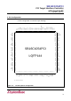
SB16C1054PCI PCI Target Interface Controller with Quad-UART JULY 2013 REV 1.04 17. Package Outline 144-Pin LQFP: Low-profile Quad Flat Package; Body 20ⅹ20ⅹ1.4 mm 0.27 0.17 1.05 MAX 1.20 MAX 0.10 0.5 17.5 20.0 22.0 Note : All dimensions are in millimeters. 74 0.75 0.45 1.