
SB16C1052PCI_Data Sheet_EN

SB16C1052PCI
PCI Target Interface Controller
with Dual UART
JULY 2013 REV 1.06
11
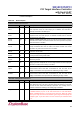
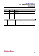
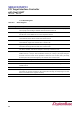
6.2 Pin Description
Table 6–1: Pin Description
Modem and Serial I/O Interface
Name
Pin
Type
Description
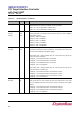
TXD0
TXD1
120
4
O
O
Transmit Data: These pins are individual transmit data output. During the
local loop-back mode, the TXD output pin is disabled and TXD data is
internally connected to the RXD input.
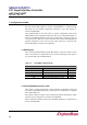
RXD0
RXD1
125
9
I
I
Receive Data: These pins are individual receive data input. During the local
loop-back mode, the RXD input pin is disabled and RXD data is internally
connected to the TXD output.
RTS0#
RTS1#
121
7
O
O
Request to Send (active low): These pins indicate that the UART is ready to
send data to the modem, and affect transmit and receive operations only when
Auto-RTS function is enabled.
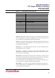
CTS0#
CTS1#
126
10
I
I
Clear to Send (active low): These pins indicate the modem is ready to
accept transmitted data from the UART, and affect transmit and receive
operations only when Auto-CTS function is enabled.
DTR0#
DTR1#
122
8
O
O
Data Terminal Ready (active low): These pins indicate UART is ready to
transmit or receive data.
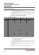
DSR0#
DSR1#
127
11
I
I
Data Set Ready (active low): These pins indicate modem is powered-on and
is ready for data exchange with UART.
DCD0#
DCD1#
128
12
I
I
Carrier Detect (active low): These pins indicate that a carrier has been
detected by modem.
RI0#
RI1#
1
13
I
I
Ring Indicator (active low): These pins indicate the modem has received a
ringing signal from telephone line. A low to high transition on these input pins
generates a modem status interrupt, if enabled.
TXEN0
TXEN1
2
14
O
O
TX Enable: These pins are for auto tri-state control of the RS422 or RS485
communication. When serial date is transmitted to TXD, the value set on
ATR[5] is transmitted. These pins eliminate additional glue logic outside.
RXEN0#
RXEN1#
3
15
O
O
RX Enable: This pins are for auto tri-state control of the RS422 or RS485
communication. When serial date is transmitted to TXD, the value set on
ATR[7] is transmitted. These pins eliminate additional glue logic outside.
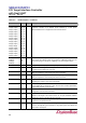
Function Configuration Interfaces
Name
Pin
Type
Description
CLKSEL
93
I
Clock Select: This pin selects the divide-by-1 or divide-by-4 prescalable
clock. During the reset, The high on CLKSEL selects the divide-by-1 prescaler.
The low on CLK selects the divide-by-4 prescaler. The inverting value of
CLKSEL is latched into MCR[7] at the trailing edge of RESET#.
ALL_EN
90
I
ALL Enable: When this pin is set, each port can be selected RS232, RS422
or RS485 interface per port. So all serial transceivers is used with RS232,
RS422 or RS485 interface in one board at the same time. When the system
boot-up, this chip check the serial interface type through the INTF0[1:0] and
INTF1[1L0] pins. If you don’t want to use ALL mode, this pin should be wired
to ‘0’.