
User Manual
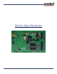
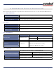
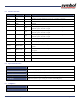
Table Of Contents

Hardware and Technical Specifications MR 100 User Manual Page: 15
MR 100 User Manual
A.5. Interface Pin Outs
Pin Number Signal Dir Description
Pin 1: VIN I Regulated +6Vdc (min/max 5.4v/7v), 1.2A max, 2A fused
Pin 2: VIN I Regulated +6Vdc (min/max 5.4v/7v), 1.2A max, 2A fused
Pin 3: GND I Ground
Pin 4: GND I Ground
Pin 5: GPIO_1
I/O
General purpose input or output #1, 3.3V TTL, configurable via board
stuff-in option, default to input.
Pin 6: GPIO_2
I/O
General purpose input or output #2, 3.3V TTL, configurable via board
stuff-in option, default to input
Pin 7: GPIO_3
I/O
General purpose input or output #3, 3.3V TTL, configurable via board
stuff-in option, default to input
Pin 8: GPO_0 O General purpose output #0, 3.3V TTL
Pin 9: GPI_0 I General purpose input #0, 3.3V TTL
Pin 10: RS-232-RxD I
RS-232 Receive Data, configurable as host interface via board stuff-in
option
Pin 11: RS-232 TxD O
RS-232 Transmit Data, configurable as host interface via board stuff-
in option
Pin 12: GND I Ground
Pin 13: TTL-RxD I 3.3V TTL Receive Data, 5V tolerant, default host interface
Pin 14: TTL-TxD O 3.3V TTL Transmit Data, 5V tolerant, default host interface
A.6. Operational Features
Frequency UHF band, 902-928 MHz
Method Frequency Hopping Spread Spectrum (FHSS); Host controlled On/Off of FH
Power Output Max 1 Watt (30 dBm, host adjustable in steps of 0.1 dB)
Read Range Typical 10’ (in free space using an antenna with 6 dBi gain)
Write Range Typical 4’ (in free space using an antenna with 6dBi gain)
A.7. Compliance
Safety EM / RF Emissions
Regulatory Region 1, FCC Part 15