SwipeSense Wireless module User Manual V1.
Introduction: (1) Use 2.4 GHz global open ISM band free license (2) The highest working rate 2Mbps, efficient GFSK modulation, anti-interference ability, especially for industrial control occasions (3) The built-in hardware CRC error detection and point to multipoint communication control. (4) Low power 1.9 - 3.6V, standby mode state is 22uA; power down mode is 900nA (5) Built in 2.
(4) 9 feet grounded, and the logical connection of the motherboard; 2 feet and 9 feet vacant. (5) gill spacing of 2.54mm, standard DIP pin, if need other package interface, such as dense feet pin, or other forms of interface can contact us custom.
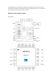
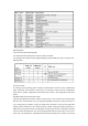
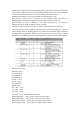
Operating mode There are four kinds of working mode: The mode of the idle mode of the transceiver mode is off mode The working mode is determined by register PRIM_RX, register PWR_UP and CE, as shown in the following table.
operating current of the whole system. In the Enhanced ShockBurstTM transceiver mode, automatic processing of NewMsg_RF24L01 prefix and CRC check code. When receiving data, automatically put the prefix and CRC check code to remove. In data transmission, automatic prefix and CRC code, in transmit mode, set the CE is high, at least 10us. When the sending process completed. Enhanced ShockBurstTM 4.1.1.1 launch process A. sends the address of the receiver and the data to send into NewMsg_RF24L01 by sequence; B.
Shockbursttm configuration word make NewMsg_RF24L01 rf24l01 to deal with RF protocol, after configuration is complete, in the process of NewMsg_RF24L01 rf24l01, only need to change the contents in the lowest one byte, the receiving and sending mode switch between. ShockBurstTM configuration word can be divided into the following four parts: Data width: the number of data occupied in the radio frequency packet.
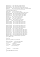
#define FLUSH_TX 0xE1 // Define flush TX register command #define FLUSH_RX 0xE2 // Define flush RX register command #define REUSE_TX_PL 0xE3 // Define reuse TX payload register command #define NOP 0xFF // Define No Operation, might be used to read status register //***************************************************// // SPI(nRF24L01) registers(addresses) #define CONFIG 0x00 // 'Config' register address #define EN_AA 0x01 // 'Enable Auto Acknowledgment' register address #define EN_RXADDR 0x02 // 'Enabled RX
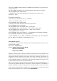
uchar status; CSN = 0; // CSN low, init SPI transaction status = SPI_RW(reg); // select register SPI_RW(value); // ..and write value to it..
//SPI_Write_Buf(WRITE_REG+RX_ADDR_P0,TX_ADDRESS,TX_ADR_WIDTH); // RX_Addr0 same as TX_Adr for Auto.Ack SPI_Write_Buf(WR_TX_PLOAD, tx_buf, TX_PLOAD_WIDTH); // Writes data to TX payload SPI_RW_Reg(WRITE_REG + CONFIG, 0x0e); // Set PWR_UP bit, enable CRC(2 bytes) & Prim:TX. MAX_RT & TX_DS enabled..
FCC RF Exposure Information and Statement This equipment complies with FCC RF radiation exposure limits set forth for an uncontrolled environment. This device complies with part 15 of the FCC rules. Operation is subject to the following two conditions: (1) this device may not cause harmful interference, and (2) this device must accept any interference received, including interference that may cause undesired operation.